Talking about the application of plasma processing technology in PCB production process, some people may still feel a little unfamiliar. I will give a brief introduction here, and hope to communicate and discuss more with PCB colleagues.
Plasma applications
Plasma processing technology is a new technology created in semiconductor manufacturing. It has been widely used in semiconductor manufacturing as early as, and it is an indispensable process for semiconductor manufacturing. Therefore, it is a long-term and mature technology in IC processing.
Because plasma is a substance with high energy and extremely high activity, it has a good etching effect on any organic materials, etc., so it has also been used in the manufacture of printed boards in recent years.
With the increasing popularity of plasma processing technology, the current main functions in the PCB manufacturing process are as follows:
(1) Hole wall erosion / Removal of resin drilling dirt on the hole wall

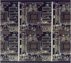
For general FR-4 multi-layer PCB manufacturing, the resin drilling and etch treatments after numerical control drilling are usually concentrated sulfuric acid treatment, chromic acid treatment, and alkaline potassium permanganate solution treatment. And plasma treatment method.
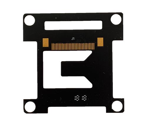
However, for flexible PCBs and rigid-flex PCBs to remove drilling contamination, due to the different characteristics of the materials, if the above-mentioned chemical treatment is used, the effect is not ideal. Plasma is used to remove drilling contamination and etchback. Better roughness of the hole wall can be obtained, which is conducive to hole metallization and electroplating, and at the same time has a "three-dimensional" etchback connection characteristic.
(2) Activation treatment of PTFE material
However, all engineers who have done the metallization of PTFE material holes have this experience: using general FR-4 multilayer PCB hole metallization manufacturing methods, it is impossible to obtain the successful PTFE printing of the hole metallization. Board. The biggest difficulty is the pretreatment of PTFE activation before electroless copper deposition, which is also the most critical step.
There are a variety of methods for the activation treatment before electroless copper deposition of PTFE materials, but in summary, to ensure product quality and suitable for batch production, there are mainly the following two methods:
(A) Chemical treatment method
"Metal sodium and naphthalene react in a solution of non-aqueous solvents such as tetrahydrofuran or ethylene glycol dimethyl ether to form a sodium naphthalene complex. The sodium naphthalene treatment solution can make the polytetrafluoroethylene surface layer atoms in the hole be etched, so as to achieve the purpose of wetting the hole wall. This is a classic and successful method with good results and stable quality. It is currently the most widely used.
(B) Plasma treatment method
This processing method is a dry process, which is easy to operate, stable and reliable in processing quality, and is suitable for mass production. As for the sodium naphthalene treatment liquid of the chemical treatment method, it is difficult to synthesize, has high toxicity, and has a short shelf life. It needs to be formulated according to the production situation and has high safety requirements.
Therefore, at present, most of the activation treatment of the polytetrafluoroethylene surface is carried out by plasma treatment, which is convenient to operate and significantly reduces waste water treatment.
(3) Carbide removal
Plasma treatment method not only has obvious effects in drilling dirt treatment of all kinds of sheets, but also shows its superiority in removing drilling dirt from composite resin materials and micro holes. In addition, with the increasing demand for higher interconnect density multilayer multilayer PCB manufacturing, a large number of laser technology is used to drill blind hole manufacturing. As a by-product of laser drilling blind hole application-carbon, It needs to be removed before the hole metallization process. At this time, the plasma treatment technology, without any denial, has taken on the important task of removing carbides.
(4) Inner pretreatment
With the increasing demand for various types of printed circuit board manufacturing, higher and higher requirements are put forward for the corresponding processing technology. Among them, the inner layer pretreatment of flexible PCB and rigid-flexible PCB can increase the surface roughness and activity, and improve the bonding force between the inner layers of the board, which is also critical for successful manufacturing.