There are three reasons for the welding defects of the PCB:
1. The solderability circuit board holes affects soldering quality
The solderability of the circuit board hole is not good, it will produce virtual soldering defects, which will affect the parameters of the components in the circuit, resulting in unstable conduction of the multi-layer board components and the inner line, causing the entire circuit to fail. The so-called solderability is the property that the metal surface is wetted by molten solder, that is, a relatively uniform continuous smooth adhesion film is formed on the metal surface where the solder is located.
The main factors that affect the solderability of printed circuit boards are:

(1) The composition of the solder and the nature of the solder. Solder is an important part of the welding chemical treatment process. It is composed of chemical materials containing flux. Commonly used low-melting eutectic metals are Sn-Pb or Sn-Pb-Ag. The impurity content must be controlled by a certain proportion, In order to prevent the oxides generated by impurities from being dissolved by the flux. The function of the flux is to help the solder wetting the circuit surface of the soldered board by transferring heat and removing rust. White rosin and isopropanol solvents are generally used.
(2) The welding temperature and the cleanliness of the metal plate surface will also affect the weldability. If the temperature is too high, the solder diffusion speed will increase. At this time, it will have a high activity, which will cause the circuit board and the molten surface of the solder to oxidize rapidly, resulting in soldering defects. Contamination on the surface of the circuit board will also affect the solderability and cause defects. These defects Including tin beads, tin balls, open circuits, poor gloss, etc.
2, welding defects caused by warpage
The circuit board and components warp during the welding process, and defects such as virtual welding and short circuit due to stress deformation. Warpage is often caused by the temperature imbalance of the upper and lower parts of the circuit board. For large PCBs, warping will also occur due to the drop of the board's own weight. The ordinary PBGA device is about 0.5mm away from the printed circuit board. If the device on the circuit board is large, the solder joint will be under stress for a long time as the circuit board cools down and the solder joint will be under stress. If the device is raised by 0.1mm, it is enough to cause Weld open circuit.
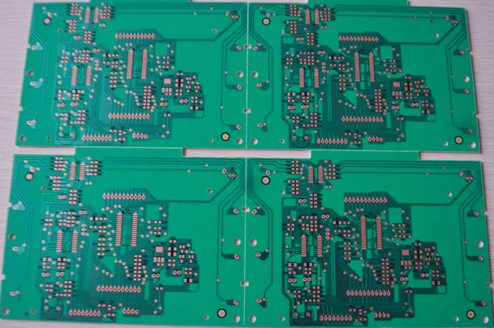
3. The design of the circuit board affects the welding quality
In the PCB layout, when the size of the circuit board is too large, although the soldering is easier to control, the printed lines are long, the impedance increases, the anti-noise ability is reduced, and the cost increases; The lines interfere with each other, such as the electromagnetic interference of the circuit board. Therefore, the PCB board design must be optimized:
(1) Shorten the connection between high-frequency components and reduce EMI interference.
(2) Components with heavy weight (such as more than 20g) should be fixed with brackets and then welded.
(3) The heat dissipation problem should be considered for heating elements to prevent defects and rework caused by large ΔT on the surface of the element, and the thermal element should be far away from the heat source.
(4) The arrangement of PCB components is as parallel as possible, which is not only beautiful but also easy to solder, and is suitable for mass production. The circuit board is best designed as a 4:3 rectangle. Do not change the wire width to avoid wiring discontinuities. When the circuit board is heated for a long time, the copper foil is easy to expand and fall off. Therefore, avoid using large-area copper foil.