PCB circuit board understands that the relevant application software is established on the PCB board machine, and the idea of virtual instrument is adopted, that is, various functions of traditional instruments are realized through software, including oscilloscope, signal generator, and various mathematical processing of collected data. During the test, a digital signal is given through the test software.
The PCB board test system will have a new design idea. The design idea of an automatic test system based on the USB bus and a virtual instrument will be adopted to give full play to the role of the computer. The idea of replacing the traditional instrument with a computer as much as possible, thereby reducing the size of the instrument The volume of itself reduces the development cost, thereby improving the efficiency of development.
After D/A conversion, the analog excitation signal required for the test is applied to the test system, and then the test circuit is sent to the switch matrix through the test bus. The switch matrix is connected to the switch matrix and controlled by the microprocessor to turn on and off. The test PCB board is fixed on the needle bed, the excitation signal is applied to the corresponding position of the printed circuit board, the response is measured by the test circuit, and the collected analog quantity is sent to the core control. After A/D conversion, the corresponding The digital quantity is fed back by the software on the PCB machine and processed by the PCB machine to determine whether the PCB board is qualified.

The online test technology has broken through the previous method of using the human eye to inspect the circuit board. The online test technology has high efficiency and low missed detection rate, and realizes the automation of the inspection field. This detection system adopts the idea of combining with virtual instruments, which reduces the design of hardware and reduces the cost of the entire system.
The basic method of on-line testing of PCB board analog components and the testing method of diodes and transistors. This testing system is suitable for the application of small and medium-sized enterprises. It reduces the number of unqualified products entering the next process, thereby reducing the amount of product rework, improving production efficiency, reducing the total cost of manufacturing, and increasing the profit of the enterprise. It is a widely used testing technology at present, and it is an efficient, High-speed, high-precision detection method.
At present, PCB boards are used in the field of automatic testing of printed circuit boards with a wide range of tests, including testing without components and testing with components. Currently, the more commonly used test methods are: continuity testing, in-circuit testing, and functional testing, Edge testing, optical testing and X-ray inspection, etc. On-line testing is based on the specific characteristics of the PCB board, selecting appropriate testing methods to combine one or more processes, complementing each other's strengths, and comprehensively using them. Because the crushing particle size is usually larger. The energy consumption in the mechanical crushing process is low. Undoubtedly, this process scheme has a broader application prospect.
Pyrolysis technology, as an efficient waste treatment and recycling method, can play an important role in the recycling of waste circuit boards. With the further in-depth research on the basic theory of pyrolysis technology and the research and development of pyrolysis equipment, it will surely become one of the most important methods for recycling circuit boards in waste electrical appliances in the future.
Although the current related research on the measurement of bromine-containing products from the pyrolysis of circuit boards is limited to qualitative analysis, or analysis based on the total amount of bromine, accurate quantitative analysis and detection of specific bromine-containing substances cannot be achieved., So it is still unable to provide enough complete information to determine the conversion and migration of bromine-containing flame retardants during the pyrolysis process.
However, many researchers have carried out some attempts to remove bromine-containing pollutants based on pyrolysis technology, and have made some breakthroughs. If you need to reprint, if you use improper technology and equipment to recycle it, the circuit board will generate more obscuring smoke, elemental bromine and hydrogen bromide gas, brominated phenol, polybrominated bibenzos during pyrolysis or combustion. Toxic and harmful substances such as dioxins/furans. These substances not only cause incalculable serious harm to the environment, but also corrode processing equipment and reduce the quality of refined oil. Therefore, whether it is from the perspective of the safe disposal of circuit boards or the recycling of circuit boards, it is necessary to have a clear understanding of the conversion and migration of bromine-containing flame retardants during the pyrolysis of circuit boards, and pay attention to the heat of waste circuit boards. Solve the problem of secondary pollution control and product debromination in the treatment process.
The circuit board condenses the pyrolyzed gas from the reactor. Obtain condensable gas and liquid pyrolysis oil. The components such as metal and glass fiber remain in the reactor to form a solid residue, and then the metal and non-metal components are separated and recovered by physical methods. The advantage of this process is that it can prevent the temperature rise caused by excessive crushing, thereby effectively avoiding the escape of toxic and harmful gases.
At present, the recycling of circuit boards is mostly based on methods that focus on the recycling of precious metals, such as pyrometallurgy and hydrometallurgy. The waste gas, waste water and waste residue produced during the treatment process can easily cause serious secondary pollution. The recycling and harmlessness of non-metallic components, which account for more than 5% of the total mass of the circuit board, involves relatively little.
Everyone can discuss it together. Here are 10 things that need to be paid attention to, and you are welcome to correct them:
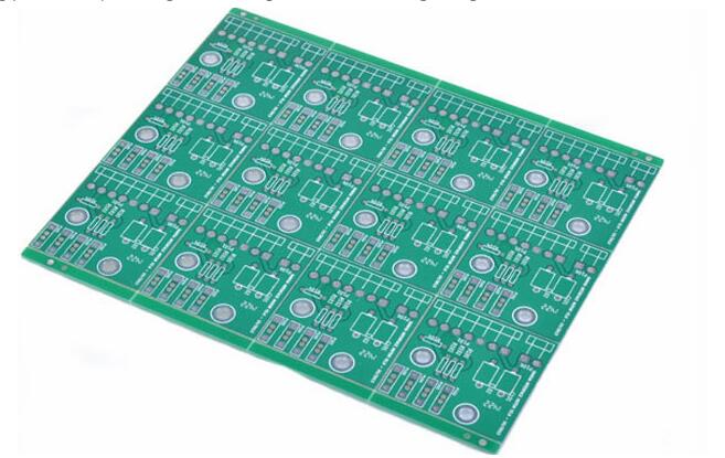
1. The outer frame (clamping side) of the PCB jigsaw should adopt a closed-loop design to ensure that the PCB jigsaw will not be deformed after being fixed on the fixture;
2. PCB panel width ≤260mm (SIEMENS line) or ≤300mm (FUJI line); if automatic dispensing is required, PCB panel width*length ≤125 mm*180 mm;
3. The shape of the PCB jigsaw should be as close to the square as possible, and 2*2, 3*3, …… jigsaw is recommended; but do not put together a yin and yang board;
4. The center distance between the small plates is controlled between 75 mm and 145 mm;
5. When setting the reference positioning point, usually leave a non-resistance area 1.5 mm larger than it around the positioning point;
6. There should be no large devices or protruding devices near the connection points between the outer frame of the jigsaw frame and the inner small board, and between the small board and the small board, and there should be a space greater than 0.5mm between the components and the edge of the PCB board. To ensure the normal operation of the cutting tool;
7. Four positioning holes are made at the four corners of the outer frame of the jigsaw panel, with a diameter of 4mm±0.01mm; the strength of the holes should be moderate to ensure that they will not break during the upper and lower boards; the precision of the hole diameter and position should be high, and the hole wall should be smooth and free of burrs. ;
8. Each small board in the PCB jigsawmust have at least three positioning holes, 3≤aperture≤6 mm, and no wiring or patching is allowed within 1mm of the edge positioning hole;
9. The reference symbols used for the positioning of the entire PCB and the positioning of fine-pitch devices. In principle, the QFP with a pitch less than 0.65mm should be set at its diagonal position; the positioning reference symbols used for the imposition PCB daughter board should be paired Used, arranged at the opposite corner of the positioning element;