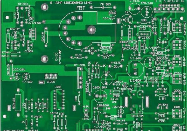
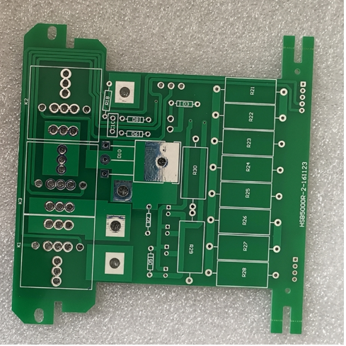
Test points generated by HDI board proofing
In a mass production factory, you can’t use an electric meter to slowly measure every resistance, capacitance, inductance, and even every HDI board proofing on every board, so there is so-called ICT (In-Circuit Test). Testing machine, which uses multiple probes (usually called "nail bed" fixtures) to simultaneously contact all the parts that need to be measured on the board, and then the characteristics of these electronic parts are controlled by the program to measure the parts in sequence with the main sequence and the side-by-side method . Generally, depending on the number of parts on the circuit board, it only takes 1-2 minutes to test all the parts on the general-purpose board., The more parts, the longer the time.
However, if these probes directly contact the electronic components or solder feet on the HDI board proofing, they may crush some electronic components, but it will be counterproductive. Therefore, there will be a test point, and the two ends of the probe will be drawn. To the round part. There is no solder mask on the small-shaped points, so the test probe can touch these small points without directly touching the electronic parts to be measured.

In the early days when there was a traditional plug-in (DIP) on the HDI board proofing, the solder feet of the parts were indeed used as test points, because the solder feet of the traditional parts were strong enough to not be afraid of acupuncture, but the probes often misjudged poor contact Because the general electronic parts are processed by wave soldering or SMT tin, a residual flux residue film is usually formed on the solder surface, and the resistance of the film is very high, which usually leads to poor contact of the probe. Therefore, at that time, I often saw test operators on the production line, who often used spray guns to blow desperately, or wipe wine in these places that needed to be tested.
However, with the development of technology, the size of HDI board proofing is getting smaller and smaller. It has been difficult to squeeze so many electronic parts on a small circuit board. Therefore, the problem of test points occupying board space is often a tug of war between the design side and the manufacturing side. The appearance of the test point is usually circular, because the probe is also circular, so it is easier to produce, and it is easier to bring adjacent probes close, which can increase the needle density of the needle bed.
iPCB is a high-tech manufacturing enterprise focusing on the development and production of high-precision PCBs. iPCB is happy to be your business partner. Our business goal is to become the most professional prototyping PCB manufacturer in the world. Mainly focus on microwave high frequency PCB, high frequency mixed pressure, ultra-high multi-layer IC testing, from 1+ to 6+ HDI, Anylayer HDI, IC Substrate, IC test board, rigid flexible PCB, ordinary multi-layer FR4 PCB, etc. Products are widely used in industry 4.0, communications, industrial control, digital, power, computers, automobiles, medical, aerospace, instrumentation, Internet of Things and other fields.