If you omit the pcb fiducial markers, you might end up in complete confusion.
What are pcb fiducial markers and how they can help manufacturing
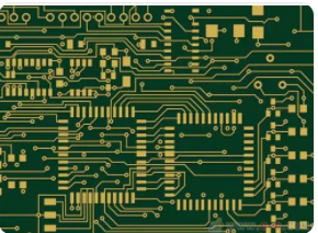
1.In PCB design, the fiducial mark is the round shape of copper, which serves as a reference point for picking and placing assembly machines. The fiducial pcb mark can help the machine identify the direction of the PCB and its surface-mounted components, using packages with small pitch, such as quad flat package (QFP), ball grid array (BGA) or quad flat no-lead (QFN).
There are two common fiducial marks in printed circuit board design: global fiducial marks and local fiducial marks. The global fiducial mark is a copper reference placed on the edge of the PCB, allowing the machine to determine the direction of the board relative to the X-Y axis. Fiducial marks are also used when placing the machine to compensate for any deflection when the PCB is clamped.
The local fiducial mark is a copper mark, located outside the corner of the surface mount component of the quad package. Assembling machines use it to accurately locate the footprint of parts and reduce errors in part placement. This is especially important when you use detailed large quad components in your design.
Always check with your manufacturer's fiducial mark requirements.
Does modern manufacturing technology require fiducial marks?
2. I have been designing my printed PCB circuit boards to have both global and local fiducial marks. However, when I saw an article explaining the possibility of omitting local benchmarks, I was very interested. It makes sense to remove the fiducial marks on the smaller PCB to maximize the signal trace space.
Due to advances in manufacturing technology, local fiducial pcb marks can be omitted under certain conditions. On smaller circuit boards, modern assembly machines can use only global reference points to place SMT components. For components with larger spacing, the fiducial mark can also be omitted. For example, the latest machines can accurately place surface mount components with a pitch greater than 1.0mm and above.
That being said, before removing local fiducial marks in your design, it is important to discuss the scope of the manufacturer's machine functions. I have learned that not all manufacturers are equipped with machines powered by the latest technology. On the other hand, never ignore the global fiducial mark in your design. Even if you are using some of the most advanced manufacturing capabilities.

3.Best practices for using fiducial marks in PCB design
If you want to get the best machine assembly, you need to get your fiducial pcb marks correct. There are few important guidelines when placing fiducial marks in a design.
The fiducial mark is made by placing an undrilled copper layer into a circle. The fiducial mark must have no solder mask.
The optimal size of the fiducial mark should be between 1mm and 3mm. A gap area similar to the diameter of the mark must be maintained.
For the global reference point, 3 markers are placed on the edge of the board for best accuracy. In the case of insufficient space, at least one global fiducials pcb mark is required.
The fiducial mark must maintain a distance of 0.3 inches from the edge of the board, excluding the clearance area of the fiducial mark.
For local fiducials, place at least two fiducial marks diagonally on the outer edge of the surface mount component.
PCB manufacturers are using professional PCB design software, such as Altium's CircuitStudio®, which can insert the pad, change the pad size to zero, and set the correct diameter value to place the pcb fiducialmarkers.