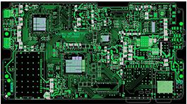
Best practices for mixed signal grounding
You know that grounding solutions usually need to be tailored specifically for mixed-signal PCBs, but there are several "best practices" that can help you solve the problem.
When designing, remember to choose the best grounding system; bus, bus or plane.
Bus: For the PCB layout design of most mixed-signal systems, the bus is not a good solution. The impedance of the bus wire can be very large at the system frequency, which can cause a large voltage drop.
Ground plane: Generally, the best solution for PCB grounding is a full ground plane. The ground plane geometry ensures the lowest possible impedance and usually provides the most direct current return path. In addition, a complete ground plane will shield the PCB more than a ground net. As with the power grid, care must be taken when connecting the integrated circuit (IC) to the PCB ground plane to ensure that the return current path does not cross. Usually, the solution is "better" and the cost is higher. If you are as frugal as Quakers, it may be worthwhile to calculate the impedance associated with the use of a bus or ground grid.
Reasonable PCB grounding design can reduce EMI in mixed-signal systems
Real grounding is not as easy as the schematic diagram.

Some mixed-signal designs may use two separate ground planes in an attempt to separate analog and digital circuits to reduce EMI. However, having two completely independent ground planes will mean that some references may be different. This may bring you errors. In circuits with a data converter, ferrite beads and Schottky diodes can be used to connect a separate ground plane. However, for more general systems, two ground planes can be combined, or one PCB ground plane can be used. As long as the AC/DC current return paths do not cross each other, it will cause "crosstalk" (just like "crosstalk" when someone cuts me off). I recommend using a solid ground plane, preferably a well-planned current return path. If a solid plane cannot be used, please cut a gap in the plane to separate the AC/DC component and its current return path. The ground plane with the gap is still continuous and will be a good reference, but will introduce a small amount of noise to the circuit. If you cut the gaps, don't leave marks on them, because the gaps can be like antennas. Regardless of the method used, please try to shorten the current return path as much as possible. This will help reduce the EMI that can be radiated by the current loop.
If there are any bypass or decoupling capacitors in the PCB design, connecting them directly to the ground plane will help reduce EMI. Grounding these capacitors quickly ensures that the path for the return current to complete the loop is very short. If the connection path between the capacitor and ground is too long, your return current may take shortcuts and eventually fall where they should not be.
Practical skills of mixed-signal IC
As you know, there are complexities in mixed-signal systems, but mixed-signal ICs may introduce more complications. Different combinations of these require different solutions. Here are some tips when dealing with mixed-signal ICs.
PCB with a single mixed signal IC
If you're familiar with the star field, we designed the audio circuit. When designing a PCB with only one mixed-signal IC, star grounding may be a good solution. The star ground uses a single point as a reference instead of the entire plane layer. For converters and other mixed-signal chips, manufacturers usually recommend connecting the AGND and DGND pins to the outside of the chip. This connection can be used as your star ground. If you use two separate ground planes and a mixed-signal IC, you can also connect the two chassis ground planes together at this point. A complication of star grounding is that the connection to star grounding needs to be as close as possible to the same length. If this configuration is not practical for your circuit, it is better to use another grounding type.
PCB with multiple mixed signal ICs
If your printed circuit board uses multiple mixed-signal ICs, star grounding is not practical. This is because you need to connect the AGND and DGND of each IC together on the outside of each IC case, all of which are in exactly the same position. William Penn didn't even plan that intersection. If you are building a PCB with multiple mixed-signal ICs on it, I recommend using a ground plane with gaps to separate the return current, or a return current path with no gaps and very careful inspection.
Hybrid-Signal system grounding requires careful layout planning because the return path needs to be checked to reduce EMI and "crosstalk." If everything looks the same, layout planning is very difficult. Use PCB design software to color-code components and networks so that the AC and DC systems or pins can be separated intuitively when using mixed-signal ICs.