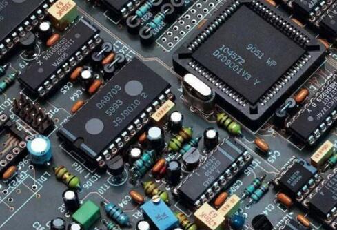
PCB boards can be divided into single-layer boards, double-layer boards, and multi-layer PCB boards. Various electronic components are integrated into the PCB. On the most basic single-layer PCB, the parts are concentrated on one side, and the wires are concentrated on the other side. In this way, we need to make holes in the board so that the pins can pass through the board to the other side, so the pins of the parts are soldered to the other side. Because of this, the front and back sides of such a PCB are respectively called PCB component side and PCB solder side.
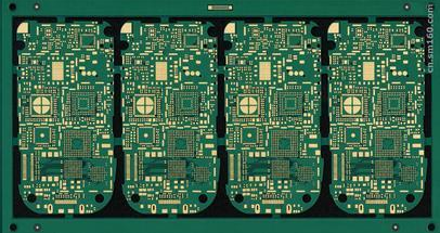
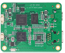
The PCB double-layer board can be regarded as a combination of two single-layer boards relative to each other. There are electronic components and wiring on both sides of the board. Sometimes it is necessary to connect a single wire on one side to the other side of the board, which requires a visa. A via is a small hole filled or coated with metal on the PCB, which can be connected with the wires on both sides. Many computer motherboards now use 4-layer or even 6-layer PCB boards, while graphics cards generally use 6-layer PCB boards. Many high-end graphics cards such as the nVIDIAGeForce4Ti series use 8-layer PCB boards. This is the so-called multi-layer PCB board. The problem of connecting the lines between the various layers will also be encountered on a multilayer PCB, which can also be achieved through vias. Because it is a multi-layer PCB board, sometimes the vias do not need to penetrate the entire PCB board. Such vias are called Buriedvias and Blindvias because they only penetrate a few layers. Blind holes are to connect several layers of internal PCB to the surface PCB, without having to penetrate the entire board. The buried via is only connected to the internal PCB, so it is invisible from the surface. In a multilayer PCB, the entire layer is directly connected to the ground wire and the power supply. So we classify the layers as a signal layer, power layer, or ground layer. If the parts on the PCB require different power supplies, this type of PCB usually has more than two layers of power and wire. The more PCB layers used, the higher the cost. Of course, the use of more layers of PCB boards is very helpful to provide signal stability.
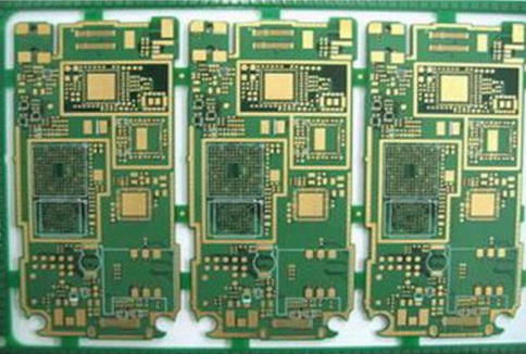
The professional PCB board production process is quite complicated, take a 4-layer PCB board as an example. The main board PCB is mostly 4-layer. When manufacturing, the two middle layers are rolled, cut, etched, and oxidized. The four layers are the component surface, power layer, ground layer, and solder pressure layer. Put these 4 layers together and roll them into a motherboard PCB. Then punch and make through holes. After cleaning, print, copper, etch, test, solder mask, silk screen on the outer two layers of circuits. Finally, the entire PCB (including many motherboards) is stamped into a motherboard PCB, and then vacuum packaged after passing the test. If the copper skin is not well laid during the PCB manufacturing process, there will be loose bonding, which may easily imply short-circuit or capacitive effects (prone to interference). The vias on the PCB must also be paid attention to. If the hole is not in the middle, but to one side, uneven matching will occur, or it will be easy to contact the power layer or ground layer in the middle, which will cause potential short circuits or poor grounding factors.

Copper wiring process
The first step is to establish the wiring between the parts. We use the negative film transfer method to express the working film on the metal conductor. This technique is to spread a thin layer of copper foil on the entire surface and eliminate the excess. The supplementary transfer is another method that fewer people use. It is a method of laying copper wires only where needed, but we won't talk about it here. A positive photoresist is made of a sensitizer, which will dissolve under lighting. There are many ways to treat the photoresist on the copper surface, but the most common way is to heat it and roll it on the surface containing the photoresist. It can also be sprayed on the head in a liquid way, but the dry film type provides higher resolution and can also produce thinner wires. The hood is just a template for the PCB layer in manufacturing. Before the photoresist on the PCB board is exposed to UV light, the light shield covering it can prevent the photoresist in some areas from being exposed. These areas covered by photoresist will become wiring. After the photoresist is developed, the other bare copper parts are to be etched. The etching process can immerse the board in the etching solvent or spray the solvent on the board. Generally used as an etching solvent, ferric chloride and the like are used. After the etching, the remaining photoresist is removed.
1. Wiring width and current
Generally, the width should not be less than 0.2mm (8mil)
On high-density and high-precision PCBs, the pitch and line width are generally 0.3mm (12mil).
When the thickness of the copper foil is about 50um, the wire width is 1~1.5mm (60mil) = 2A
The common area is generally 80mil, and more attention should be paid to applications with microprocessors.
2. How high is the frequency of a high-speed PCB board?
When the rising/falling edge time of the signal is less than 3~6 times the signal transmission time, it is considered as a high-speed signal.
For digital circuits, the key is to look at the steepness of the signal edge, that is, the rise and fall time of the signal.
According to the theory of a very classic book, High-Speed Digital Design the time for the signal to rise from 10% to 90% is less than 6 times the wire delay, which is a high-speed signal!
-That is, even an 8KHz square wave The signal, as long as the edge is steep enough, is also a high-speed signal, and transmission line theory needs to be used when wiring.
3. Precautions for the power cord and ground wire layout
The power cord should be as short as possible, in a straight line, and preferably in a tree shape rather than a loop.
Ground loop problem: For digital circuits, the ground loop caused by ground loops is tens of millivolts, while the anti-interference threshold of TTL is 1.2V, and CMOS circuits can reach 1/2 power supply voltage., That is to say, the circulation of ground wire will not cause adverse effects on the operation of the circuit at all. On the contrary, if the ground wire is not closed, the problem will be even greater, because the pulse power current generated by the digital circuit when it is working will cause the ground potential of each point to be unbalanced. Measured by a 2Gsps oscilloscope, the ground current pulse width is 7ns). Under the impact of a large pulse current, if a branch ground wire (line width 25mil) is used, the potential difference between the ground wires will reach the level of 100 millivolts.
After the ground loop is adopted, the pulse current will be scattered to various points of the ground wire, which greatly reduces the possibility of interference with the circuit. Using a closed ground wire, the measured maximum instantaneous potential difference between the ground wires of each device is one-half to one-fifth of the unclosed ground wire. Of course, the measured data of circuit boards with different densities and speeds are very different. What I said above is about the level of the Z80 Demo board attached to the Protel 99SE; for the low-frequency PCB analog circuit, I think the work after the ground wire is closed Frequency interference is induced from space, which cannot be simulated and calculated anyway. If the ground wire is not closed, the ground wire eddy current will not be generated. Beckhamtao's so-called "but the power frequency induced voltage of the ground wire will be larger." The project, the precision pressure gauge, uses a 14-bit A/D converter, but the actual measurement only has an effective accuracy of 11 bits. After investigation, there is 15mVp-p power frequency interference on the ground line.
The solution is to use the analog ground loop of the PCB board After dividing, the ground wire from the front-end sensor to the A/D is distributed in a branch with flying leads. Later, the mass-produced model PCB is reproduced according to the flying leads, and there is no problem so far. In the second example, a friend loves to have a fever and DIYs an amplifier by himself, but there is always a humming sound at the output. I suggest that it cut the ground loop to solve the problem. Afterwards, this man consulted dozens of "Hi-Fi famous machines" PCB diagrams and confirmed that none of the machines used ground loops in the analog part.