PCB copy board, the industry is often referred to as circuit board copy board, circuit board clone, circuit board copy, PCB clone, PCB reverse design or PCB reverse development.
Reverse step
1. Record the relevant details of PCB copy board
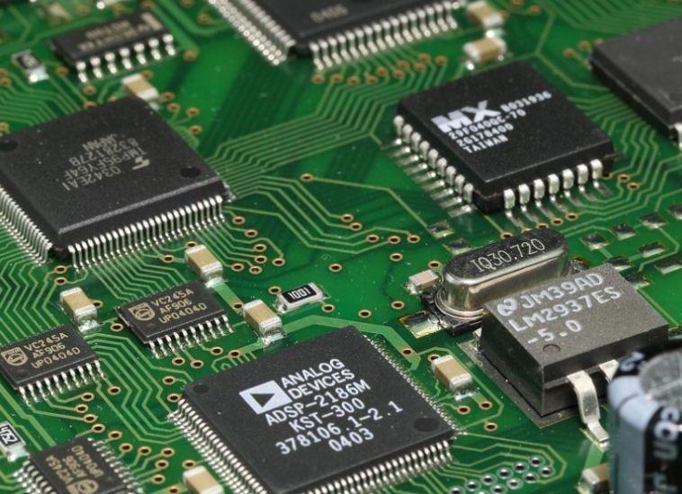
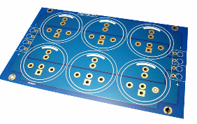
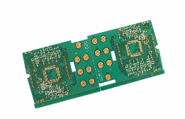
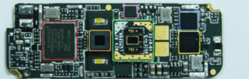
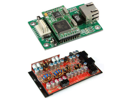
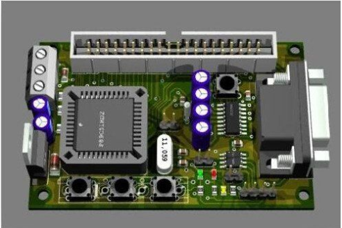
Get a PCB copy board, first record the model, parameter, and position of all the components on the paper, especially the direction of the diode, the tertiary tube, and the direction of the IC gap. It is best to use a digital camera to take two photos of the location of the components. Many PCB copy board circuit boards are getting more and more advanced. Some of the diode transistors on the above are not noticed and can't be seen at all.
2. Scanned image
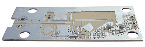
Remove all components and remove the tin in the PAD hole. Clean the PCB copy board with alcohol, and then put it into the scanner. When the scanner scans, you need to raise the scanned pixels slightly to get a clearer image.

Then lightly polish the top and bottom layers with water gauze until the copper film is shiny, put them in the scanner, start PHOTOSHOP, and scan the two layers in separately in color.
Note that the PCB copy board must be placed horizontally and vertically in the scanner, otherwise the scanned image cannot be used.
3. Adjust and correct the image
Adjust the contrast and brightness of the canvas to make the part with copper film and the part without copper film have a strong contrast, then turn the second image into black and white, and check whether the lines are clear. If not, repeat this step. If it is clear, save the picture as black and white BMP format files TOP BMP and BOT BMP. If you find any problems with the graphics, you can also use PHOTOSHOP to repair and correct them.
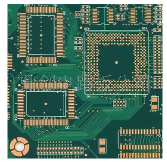
4. Verify the positional coincidence of PAD and VIA
Convert the two BMP format files to PROTEL format files, and transfer them into two layers in PROTEL. For example, the positions of PAD and VIA that have passed through the two layers basically coincide, indicating that the previous steps have been done well. If there is a deviation, then Repeat the third step. Therefore, PCB copying is a work that requires patience, because a small problem will affect the quality and the degree of matching after copying.
5. Draw the layer
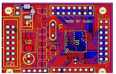
Convert the BMP of the TOP layer to the TOP PCB, pay attention to the conversion to the SILK layer, which is the yellow layer, and then you can trace the line on the TOP layer, and place the device according to the drawing in the second step. Delete the SILK layer after drawing. Repeat until all the layers are drawn.
6. TOP PCB and BOT PCB combined picture
Import TOP PCB and BOT PCB in PROTEL and combine them into one picture.
7. Laser printing TOP LAYER, BOTTOM LAYER
Use a laser printer to print the TOP LAYER and BOTTOM LAYER on the transparent film (1:1 ratio), put the film on the PCB, and compare whether there is any error. If it is correct, you are done.
8. Test
Test whether the electronic technical performance of the copy board is the same as the original board. If it is the same, it is really done.