PCB copy board design and manufacturing is moving from subtractive method to additive method. This article mainly explains the related concepts and manufacturing process of PCB subtractive method for your reference and learning!
1. Introduction to PCB Subtractive Process
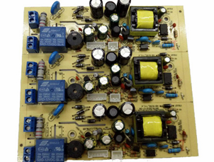
The subtractive process is a method of selectively removing part of the copper foil on the surface of the copper-clad laminate to obtain a conductive pattern. The subtractive method is the main method of PCB manufacturing today, and its biggest advantage is that the process is mature, stable and reliable.
PCB circuits manufactured by the subtractive process can be divided into the following two categories.
1. Non-porous printed circuit board (. Non-plating-thr’ough-hole Board)

This type of printed board is produced by screen printing and then the printed board is etched out, or it can be produced by photochemical method. The non-perforated plated printed boards are mainly single-sided boards, but also a few double-sided boards, which are mainly used for televisions and radios. The following is the single-sided production process:
Single-sided copper-clad board: unloading-photochemical method/screen printing image transfer-removing resist printing-cleaning and drying-hole processing-shape processing-cleaning and drying-printing solder mask coating-curing-printing marking symbol- Curing-cleaning and drying-pre-coating flux-drying-finished product.
2. Plating-through-hole Board
On the copper clad laminates that have been drilled, electroless plating and electroplating are used to electrically insulate the pores between two or more conductive patterns into electrical connections. This type of printed board is called perforated plating. Printed board. Perforated plated printed boards are mainly used in computers, program-controlled switches, mobile phones, etc. According to the different electroplating methods, it is divided into pattern electroplating and full plate electroplating.
(1) Pattern plating (Patter.n, P'I'N) On double-sided copper clad laminates, conductive patterns are formed by screen printing or photochemical methods, and lead-tin, tin-cerium are plated on the conductive patterns, Tin-nickel or gold and other anti-corrosive metals, and then remove the resist other than the circuit pattern, and then be formed by etching. The pattern plating method is divided into pattern plating etching process (Pattern PlATIng And Etching Process) and bare copper covered solder mask process (Solder Mask OnBare Copper, SMOBC). The process of making double-sided PCB boards with bare copper-clad solder mask process is as follows.
Double-sided copper clad laminates are blanked, positioning holes, CNC drilling, inspection, hair removal, electroless thin copper plating, thin copper electroplating, inspection, brushing, filming (or screen printing), exposure and development (or curing), Inspection and repairing a pattern copper plating a pattern tin-lead alloy plating a film removal (or removal of the printing material) a inspection and repairing a pattern etching a lead tin removal a circuit test-cleaning a solder mask pattern a plug nickel/gold plating a plug paste Adhesive tape-hot air leveling-cleaning-screen printing marking symbols-shape processing-cleaning and drying-inspection-packaging-finished product.
(2) Full board plating (Panel, PNL) On double-sided copper clad laminates, plating
Copper to the specified thickness, and then use screen printing or photochemical method for image transfer to obtain a corrosion-resistant normal-phase circuit image, after etching and then remove the resist to make a printed board.
The whole plate electroplating method can be subdivided into the plugging method and the masking method. The process flow of making double-sided printed boards with the masking method (TenTIng) is as follows.
Double-sided copper clad laminates are cut, drilled, L, metalized, full-board plating, thickened, surface treatment, pasted, photomasked, dry film, positive-phase wire pattern, etched, removed, plug plating, shape Processing-inspection-printing of solder mask-solder coating hot-air leveling-printing of marking symbols-finished products.
The advantages of the above method are simple process and good uniformity of coating thickness. The disadvantage is that it is a waste of energy, and it is difficult to manufacture a through-hole PCB circuit board without a land.