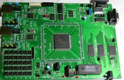
Hybrid circuit PCB design is a complex process. The layout and wiring of components and the processing of power and ground wires will directly affect the circuit performance and electromagnetic compatibility. When designing, follow certain wiring rules to make the designed PCB board reach Design requirements.
The faster the speed of the digital circuit, the shorter the switching time is generally required. When a large number of switching circuits change from a logic high level to a logic low level at the same time, due to the insufficient ability of the ground wire to pass current, a large amount of switching current will be caused. The logic ground voltage fluctuates, which we call ground bounce. The ground bounce noise and power disturbance caused by the digital circuit, if coupled to the analog circuit, will affect the performance of the analog circuit. Since quite a lot of interference sources are generated through the power and ground buses, the ground wire causes the largest noise interference, so the design of the ground and power is particularly important in the PCB design.

I talked about the mechanism of hybrid circuit interference. How to reduce the mutual interference between digital signal and analog signal? Before designing, you must understand the two basic principles of electromagnetic compatibility (EMC): The first principle is to reduce the area of the current loop as much as possible. If the signal cannot return through the smallest possible loop, a large loop may be formed.状 Antenna. The second principle is that the system uses only one reference plane. On the contrary, if the system has two reference planes, it may form a dipole antenna. Avoid these two situations as much as possible in the design.
(1) PCB layout and wiring principles. One of the first factors to consider for component layout is to separate the analog circuit part from the digital circuit part. The analog signal is routed in the analog area of all layers of the circuit board, and the digital signal is routed in the digital circuit area. In this case, the digital signal return current will not flow into the analog signal ground. For some high-frequency lines with special requirements, it is best to manually route them, and use differential lines or shielded lines when necessary. Sometimes due to the position of the input/output connector, the wiring of the digital and analog circuits must be mixed together, which may cause the mutual influence of the analog part and the digital part of the circuit. This is necessary to avoid running digital clock lines and high-frequency analog signal lines near the analog power layer, otherwise, the noise of the power signal will be coupled to the sensitive analog signal. To try to achieve a low-impedance power and ground network, the inductance of the digital circuit wire should be minimized, and the capacitive coupling of the analog circuit should be minimized. The frequency of the digital circuit is high, and the sensitivity of the analog circuit is strong. For the signal line, the high-frequency digital signal line should be as far away as possible from the sensitive analog circuit device.
(2) Treatment of power and ground. In the design of complex hybrid PCB circuit boards, the layout and handling of grounding wires are important factors to improve circuit performance. It is suggested to separate the digital ground and analog ground on the mixed-signal circuit board to achieve isolation between the digital ground and the analog ground. However, this method tends to cross the separation gap wiring, which will cause a sharp increase in electromagnetic radiation and signal crosstalk.