PCB board plug hole introduction
Conductive holes are also known as vias. In order to meet customer requirements, the PCB board vias must be plugged. After a lot of practice, the traditional aluminum plugging process is changed, and the PCB board surface soldering and plugging are completed with white mesh. Stable production and reliable quality.

via holes play the role of interconnection and conduction of lines. The development of the electronics industry also promotes the development of PCB, and also puts forward higher requirements on the PCBboard manufacturing process and surface mount technology.
plug hole technology came into being, and should meet the following requirements at the same time:
(A) There is copper in the through hole, and the solder mask can be plugged or not plugged;
(2) There must be tin-lead in the via hole, with a certain thickness requirement (4 microns), and no solder mask ink can enter the hole, causing tin beads to be hidden in the hole;
(3) The through holes must have solder mask ink plug holes, opaque, and must not have tin rings, tin beads, and flatness requirements.
The benefits of circuit board plug holes
(1) Prevent the tin from passing through the via hole to cause a short circuit when the PCB is wave soldered; especially when we put the via on the pad, we must first plug the hole and then gold-plated for easy soldering.
(2) Avoid flux residue in the via;
(3) After the surface mounting and component assembly of the electronics factory are completed, the PCB must be vacuumed on the testing machine to form a negative pressure to complete:
(four) to prevent surface solder paste from flowing into the hole, causing false soldering, affecting placement;
(5) Prevent the solder balls from popping up during wave soldering, causing short circuits.
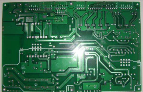
The composition of the circuit board
PCB circuit board is mainly composed of pads, vias, mounting holes, wires, components, connectors, filling, electrical boundaries, etc. The main functions of each component are as follows:
Pad: A metal hole used to solder the pins of components.
Via: A metal hole used to connect the pins of components between layers.
Mounting hole: used to fix the printed circuit board.
Wire: The copper film of the electrical network used to connect the pins of the components.
Connectors: used to connect components between circuit boards.
Filling: used for copper coating of the ground wire network, which can effectively reduce the impedance.
Electrical boundary: used to determine the size of the PCB board, all components on the circuit board cannot exceed the boundary.
PCB board layer classification
The common layer types of printed circuit board include single layer PCB, double layer PCB, and multilayer PCB. A brief description of the three layer structures is as follows:

(1) Single layer board:
is a circuit board with copper on one side and no copper on the other side. Usually components are placed on the side without copper, and the side with copper is mainly used for wiring and soldering.
(2) Double-layer board:
is a PCB board with copper on both sides, usually called the top layer on one side and the bottom layer on the other side. Generally, the top layer is used as the surface for placing components, and the bottom layer is used as the welding surface for components.
(3) Multilayer board:
is a PCB board that contains multiple working layers. In addition to the top and bottom layers, it also contains several intermediate layers. Usually the intermediate layers can be used as wire layers, signal layers, power layers, ground layers, etc. The layers are insulated from each other, and the connection between the layers is usually achieved through vias.