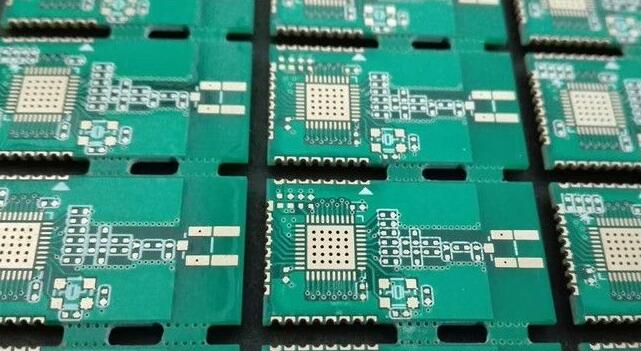
At present, many people think that the PCB manufacturing process is super complicated and difficult to understand, but the work needs are not understood or not. What should I do? You can directly contact Wanlong Lean to undertake the production of multi-layer circuit boards. Let me let the editor let you easily get the tips of multi-layer PCB production. Don't think this is too difficult! Do not believe it, continue to read below:
At present, PCB manufacturing is mostly a subtractive method, that is, the excess copper foil on the raw material copper clad board is subtracted to form a conductive pattern.
The method of subtraction is mostly chemical corrosion, which is the most economical and efficient. Only chemical corrosion does not attack, so it is necessary to protect the required conductive pattern. A layer of resist must be coated on the conductive pattern, and then the unprotected copper foil is corroded and subtracted.

In the early days of resist, the resist ink was printed in the form of a circuit by screen printing, so it was called "printed circuit". However, as electronic products become more and more sophisticated, the image resolution of the printed circuit cannot meet the product requirements, and then photoresist is used as an image analysis material.
Photoresist is a photosensitive material that is sensitive to a certain wavelength of light source and forms a photochemical reaction with it to form a polymer. It only needs to use a pattern film to selectively expose the pattern, and then pass it through a developer solution (example 1% carbonic acid) Sodium solution) strips off the unpolymerized photoresist to form a patterned protective layer.
In addition, the interlayer conduction function is realized through metallized holes, so drilling operations are required during the PCB manufacturing process, and the holes are metallized and electroplated, and finally interlayer conduction is realized.
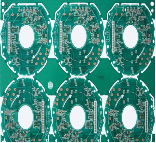
The production process of a conventional 6-layer circuit board in a nutshell:
One: First make two non-porous double panels:
Cutting (raw material double-sided copper clad laminate)-inner layer pattern production (form pattern resist layer)-inner layer etching (minus excess copper foil)
Two: The two inner core boards are glued and pressed together with epoxy resin glass fiber prepreg
The two inner core boards and the prepreg are riveted together, and then a piece of copper foil is laid on both sides of the outer layer and pressed under high temperature and high pressure with a press to make them adhered and combined. The key material is a prepreg. The composition is the same as that of the original material. It is also epoxy resin glass fiber, but it is not fully cured and will liquefy at a temperature of 7-80 degrees. A curing agent is added to it, and it will cross with the resin at 150 degrees. The linked reaction solidifies and is no longer reversible afterwards. Through such a semi-solid-liquid-solid conversion, adhesive bonding is completed under high pressure.
Three conventional PCB double-sided production
Drilling-Immersion copper plate electricity (hole metallization)-Outer circuit (forming patterned resist layer)-Outer layer etching-Solder mask (printing green oil, text)-Surface coating (tin spraying, immersion gold, etc.)-Forming (Milling to shape), done!