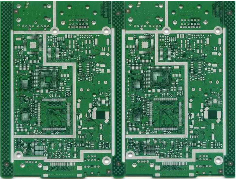
Printed circuit board (PCB) is almost present in every kind of electronic device. If there are electronic parts in a certain device, they are all mounted on PCBs of different sizes. In addition to fixing various small parts, the main function of PCB is to provide electrical connection between the upper parts. As electronic devices become more and more complex, more and more parts are required, and the circuits and parts on the PCB are becoming more and more dense. The standard PCB looks like this. The bare board (no parts on it) is also often called "Printed Wiring Board (PWB)".
The base plate of the board itself is made of insulating and heat-insulating materials that are not easy to bend. The small circuit material that can be seen on the outside is copper foil. The copper foil was originally covered on the entire board, but part of it was etched away during the manufacturing process, and the remaining part became a network of small lines. . These lines are called conductor patterns or wiring, and are used to provide circuit connections for parts on the PCB.

In order to fix the parts on the PCB, we solder their pins directly on the wiring. On the most fundamental PCB (single panel), the parts are concentrated on one side, and the wires are concentrated on the other side. In this way, we need to make holes in the board so that the pins can pass through the board to the other side, so the pins of the parts are soldered to the other side. Because of this, the front and back sides of the PCB are called Component Side and Solder Side respectively.
If there are certain parts on the PCB that need to be removed or reinstalled after the manufacturing is completed, then the socket will be used when the part is installed. Since the socket is directly welded to the board, the parts can be disassembled and assembled at will. What you see below is the ZIF (Zero Insertion Force) socket, which allows parts (here refers to the CPU) to be easily inserted into the socket and can also be removed. The fixing rod next to the socket can fix it after you insert the part.
If you want to connect two PCBs to each other, we usually use an edge connector commonly known as "golden finger". There are many exposed copper pads on the golden fingers, which are actually part of the PCB wiring. Usually, when connecting, we insert the golden fingers on one PCB into the appropriate slot on the other PCB (commonly called the expansion slot Slot). In computers, display cards, sound cards or other similar interface cards are connected to the motherboard by means of golden fingers.
The green or brown on the PCB is the color of the solder mask. This layer is an insulating protective layer, which can maintain the copper wire and prevent the parts from being welded to the incorrect center. A layer of silk screen will be printed on the solder mask. Usually words and symbols (mostly white) are printed on this to mark the position of each part on the board. The screen printing surface is also called the legend surface.
Single-Sided Boards
We just mentioned that on the most fundamental PCB, the parts are concentrated on one side, and the wires are concentrated on the other side. Since the wires are only present on one side, we call this kind of PCB a single-sided (Single-sided). Because single-sided boards have many severe restrictions on the design of the circuit (because only one side, the wiring can not be interspersed and must go around a separate path), so only early circuits use this type of board.
Double-Sided Boards
This kind of circuit board has wiring on both sides. However, to use wires on both sides, you must have a proper circuit connection between the two sides. This kind of "bridge" between circuits is called a via. A via is a small hole filled or coated with metal on the PCB, which can be connected with the wires on both sides. Since the area of the double-sided board is twice as large as that of the single-sided board, and because the wiring can be interwoven (can be wound to the other side), it is more suitable for use in circuits that are more complicated than the single-sided board.
Multilayer Boards
In order to increase the area that can be wired, multilayer boards use more single or double-sided wiring boards. The multi-layer board uses several double-sided boards, and a layer of insulating layer is placed between each board and then glued (press-fitted). The number of layers of the board means that there are several independent wiring layers. Usually the number of layers is even and contains the two outermost layers. Most of the motherboards are constructed with 4 to 8 layers, but technically it is possible to achieve nearly 100 layers of PCB board. Large-scale supercomputers mostly use very multi-layer motherboards. However, since these types of computers have been able to be replaced by clusters of many ordinary computers, super-multilayer boards have been slowly not used. Since the layers in the PCB are tightly separated, it is not easy to see the actual number, but if you look at the motherboard carefully, you may be able to see it.