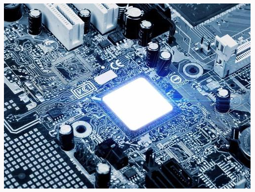
The etching process is one of the basic steps in the PCB production process. Simply put, the base copper is covered by the resist layer, and the copper that is not protected by the resist layer reacts with the etchant, which is bitten off, and finally forms the design circuit pattern and The process of bonding pads. Of course, the principle of etching can be easily described in a few sentences, but in fact, the realization of etching technology is still quite challenging, especially in the production of fine lines, which requires very small line width tolerances and does not allow any errors in the etching process., So the etching result should be just right, it can't be widened, and it can't be over-etched.
To further explain the etching process, PCB manufacturers are more willing to use horizontal etching lines for production to achieve maximum production automation and reduce production costs. However, horizontal etching is not perfect, and the "pool effect" that cannot be eliminated makes the board difficult. The upper surface and the lower surface produce different etching effects. The etching rate at the edge of the board is faster than the etching rate at the center of the board. Sometimes, this phenomenon can make the etching results on the board surface quite different.
In other words, the "pool effect" will make the over-corrosion of the circuit on the edge of the board larger than that in the center of the board, and even careful circuit correction (appropriately widening the circuit width on the edge of the board) to compensate for different etching The rate will also fail, because the etching tolerances must be very finely controlled to obtain ultra-fine lines.
This situation leads to significant changes in the etching rate. Located on the circuit board, near the edge of the board, the etching solution is more likely to flow out of the board, and the old and new etching solutions are easier to exchange, so a good etching rate is maintained. In the center of the board, it is easier to form a "pool" situation, and the flow of the etchant is therefore restricted. It is relatively difficult for the solution rich in copper ions to flow out of the board surface. As a result, the etching efficiency is reduced compared with the edge or the underside of the board. The etching effect becomes worse. In fact, it is impossible to avoid the "pool effect" in practice, because the chain-type horizontal transmission rollers will prevent the discharge of the etching liquid, resulting in the accumulation of the etching liquid between the rollers.

This phenomenon occurs in the production of larger plates. Or ultra-fine lines are more obvious, even if more special production process control and compensation methods are used, such as a spray system that can be adjusted independently of the transmission direction, an oscillating spray pipe and a corrective re-etching section Wait, if there is no huge technical investment, this problem can not be solved well, so the goal of avoiding the "pool effect" is achieved without having to go back to the starting point and start again.
At the end of last year, PILL e.K. released a new process technology, which can improve the fluidity of the etching solution on the upper part of the board by simply sucking the used etching solution through a water pump, thereby preventing the puddle effect. This method is called vacuum etching.
The first vacuum etching line was demonstrated to the public at Productronica in November 2001. At the same time, the test conducted by the circuit board manufacturer also confirmed that the vacuum etching process can achieve excellent results only with less effort to control the engineering conditions.
After vacuum etching, the etching effect is very uniform on the entire surface of both sides of the board.
The principle of vacuum etching technology is very simple. Not only are nozzles installed in the etching section, but also an air extraction unit is installed between the nozzles at a relatively close distance to the surface of the circuit board. After these pumping units suck away the used etching solution, they return to the liquid tank of the module through a closed loop.
Here, the vacuum refers to the negative pressure in the operating area of the system and the low suction just enough to prevent the etchant from producing a puddle effect. Even the thinnest inner layer cannot be sucked up by the suction unit, and the production accuracy needs to be guaranteed. By connecting the track of the aspirator to the upper fixed reel in the conveyor system, the designer ensures that the distance between the pumping process and the board surface is the best value, regardless of whether the production is thin or thick. This means that no matter what type of PCB board, a uniform etching solution extraction rate can be obtained. On the entire surface of the 24"X24" large board, on the upside of the circuit board, only 1 micron copper thickness fluctuations were found. By comparison, the etching effect of the upward part and the downward part of the plate is basically the same.
The circuit quality of the production board using vacuum etching technology is also very good. Detailed tests conducted with different PCB manufacturers have shown that the new vacuum etching technology can produce straighter conductor profiles so that the produced boards can more accurately approach the wiring requirements.
In the vacuum etching process, the shrinkage rate of the etching medium under the resist film on the side attack of the wire and the etching factor used to describe the wire etching depth and the side etching amount are very high.
Of course, there are also a series of other factors that are basically not affected by the manufacturer that will affect the actual etching effect. For example, the thickness of the resist, the quality of the exposure and development process, and the copper thickness of the etched substrate each have a large impact. In general, it is estimated that the etching process or the renewal frequency of the etching solution only accounts for half of the etching effect. . But Oliver Briel, the PILL project manager, emphasized that "the facts have proved that we have completely controlled this 50%."
vacuum etching technology also shows a series of advantages in other aspects:
can make full use of the capacity of the etching process. As the etching speed increases and the production time is shortened, the output of the etching process increases.
Since the first etching can achieve satisfactory results, there is no need to rework and re-etch.
can reduce the related factory control engineering and reduce the corresponding cost.
The vacuum etching system uses relatively simple technology to produce ultra-fine wires, and no longer need to install a swingable jet manifold.
The nozzle structure with intermittently adjustable spray pressure can no longer be used. This design is mainly used to ensure that the puddle effect is reduced, which can now be accomplished simply by using an air suction system.
PCB vacuum etching technology allows the process module to be shorter and tighter, and the functions of suction and etching can be completed simultaneously in the same module.
The additional advantage of the vacuum etching technology system is that the injection manifold can be arranged laterally along the direction of travel. Conventional spray manifolds used for the production of fine wire boards usually need to be arranged longitudinally along the direction of travel so that different spray pressures can exist on the edge of the board and in the board. The angle between the nozzle and the direction of travel is appropriate to facilitate maintenance and requires less time for replacement, and this arrangement method can also perform simple electrical flow monitoring for each injection manifold individually. If there is an irregular situation, the user can immediately identify which injection manifold has the problem, and then can directly adjust it without delay.
PCB vacuum etching technology has great potential in the future, because the process is particularly suitable for the production of thin wires and ultra-fine wire structure boards. Preliminary tests on conductive patterns below 50 microns can get promised results. The ability to use vacuum etching technology to produce thick copper circuits is being further evaluated, and all current data show that the results are good. It is particularly noteworthy that not only the traditional copper chloride was used as the etching medium during the test, but also the iron chloride (3), which is currently commonly used in Asia, was also used as the etching medium. Although it takes a long time to use this etching medium, the effect is better when the conductor profile is steeper, and it undoubtedly provides an alternative to the process that has been accepted as a standard, especially for special features. Production of fine lines.