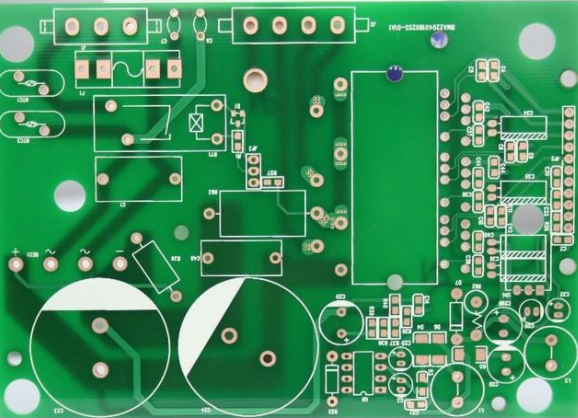
1. How to consider impedance matching when designing high-speed PCB design schematics?
When designing high-speed PCB circuits, impedance matching is one of the design elements. The impedance value has an absolute relationship with the wiring method, such as walking on the surface layer (microstrip) or inner layer (stripline/double stripline), distance from the reference layer (power layer or ground layer), wiring width, PCB material, etc. Both will affect the characteristic impedance value of the trace. That is to say, the impedance value can only be determined after wiring. Generally, simulation software cannot take into account some wiring conditions with discontinuous impedance due to the limitation of the circuit model or the mathematical algorithm used. At this time, only some terminators (termination), such as series resistance, can be reserved on the schematic diagram. Alleviate the effect of discontinuity in trace impedance. The real way to solve the problem is to try to avoid impedance discontinuity when wiring.
2. When there are multiple digital/analog function blocks in a PCB board, the conventional method is to separate the digital/analog ground. What is the reason?
The reason for separating the digital/analog ground is because the digital circuit will generate noise on the power supply and ground when switching between high and low potentials. The magnitude of the noise is related to the speed of the signal and the magnitude of the current. If the ground plane is not divided and the noise generated by the digital area circuit is relatively large and the analog area circuits are very close, the analog signal will still be disturbed by the ground noise even if the digital-to-analog signals do not cross. That is to say, the undivided digital-to-analog ground method can only be used when the analog circuit area is far from the digital circuit area that generates large noise.
3. In high-speed PCB design, which aspects should the designer consider the EMC and EMI rules?

Generally, EMI/EMC design needs to consider both radiated and conducted aspects at the same time. The former belongs to the higher frequency part (>30MHz) and the latter is the lower frequency part (<30MHz). So you can't just pay attention to the high frequency and ignore the low frequency part. A good EMI/EMC design must take into account the location of the device, PCB stack arrangement, important connection method, device selection, etc. at the beginning of the layout. If there is no better arrangement beforehand, it will be resolved afterwards. It will do twice the result with half the effort and increase the cost. For example, the location of the clock generator should not be as close to the external connector as possible. High-speed signals should go to the inner layer as much as possible. Pay attention to the characteristic impedance matching and the continuity of the reference layer to reduce reflections. The slew rate of the signal pushed by the device should be as small as possible to reduce the height. Frequency components, when choosing decoupling/bypass capacitors, pay attention to whether the frequency response meets the requirements to reduce noise on the power plane. In addition, pay attention to the return path of high-frequency signal current to make the loop area as small as possible (that is, loop impedance as small as possible) to reduce radiation. The ground can also be divided to control the range of high-frequency noise. Finally, properly choose the chassis ground between the PCB and the case.
4. When making PCB boards, in order to reduce interference, should the ground wire form a closed sum form?
When making PCB boards, the loop area is generally reduced in order to reduce interference. When laying the ground line, it should not be laid in a closed form, but it is better to arrange it in a branch shape, and the area of the ground should be increased as much as possible.
5. How to adjust the routing topology to improve signal integrity?
This kind of network signal direction is more complicated, because for unidirectional, bidirectional signals, and signals of different levels, the topology influences are different, and it is difficult to say which topology is beneficial to the signal quality. In addition, during the pre-simulation, which topology to adopt is very demanding on the engineer, it is required to understand the circuit principle, signal type, and even the difficulty of wiring.
6. How to deal with PCB layou t and wiring to ensure the stability of signals above 100M?
The key to high-speed digital signal wiring is to reduce the impact of transmission lines on signal quality. Therefore, the layout of high-speed signals above 100M requires the signal traces to be as short as possible. In digital circuits, high-speed signals are defined by signal rise delay time. Moreover, different types of signals (such as TTL, GTL, LVTTL) have different methods to ensure signal quality.