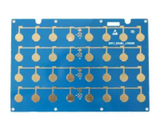
PCB assembly skills 1
The selective soldering process includes: flux coating, board preheating, dip soldering and drag soldering. In the selective soldering process, the flux coating process plays an important role. At the end of solder heating and soldering, the flux should have sufficient activity to prevent bridging and prevent oxidation of the circuit board. The flux is sprayed by the X/Y robot carrying the circuit board through the flux nozzle, and the flux is sprayed to the soldering position of the PCB board.
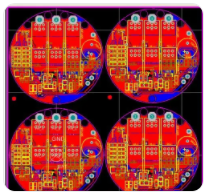
PCB assembly skills 2
The most important thing for the microwave peak after the reflow soldering process is the accurate spraying of the flux, and the micro-hole spray type will never contaminate the area outside the solder joint. The minimum solder pattern diameter of micro-spraying is greater than 2mm, so the solder placement accuracy of the solder deposited on the circuit board is ±0.5mm to ensure that the flux channel covers the soldered part.
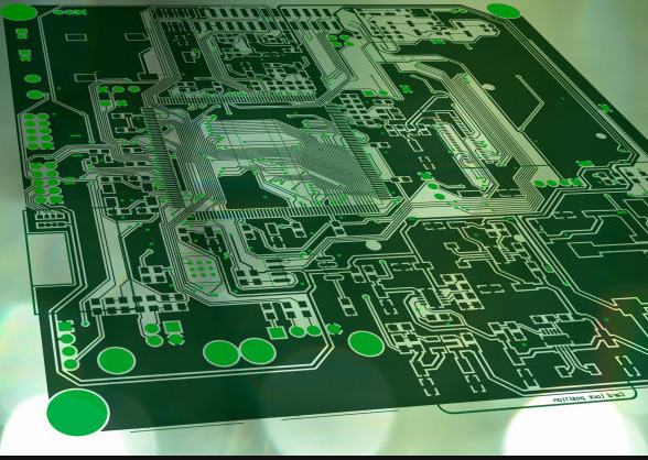
PCB assembly skills 3
By comparing with wave soldering, the characteristics of selective soldering can be understood. The most obvious difference between the two is that the lower part of the wave soldering board is completely immersed in liquid solder. In selective soldering, only some specific areas are in contact with the solder wave. Since the circuit board itself is a poor heat transfer medium, the solder joints of adjacent components and the circuit board area will not be heated and melted during the soldering process.

The flux must also be pre-coated and soldered in advance. Compared with wave soldering, flux is only applied to the part of the board to be soldered, not the entire PCB board. In addition, selective soldering is only suitable for soldering inserted components. Selective welding is a completely new method that is necessary to fully understand the selective welding process and equipment that is necessary for successful welding.
Precautions for PCB board welding
1. After obtaining the bare PCB, first check the appearance to see if there is a short circuit or an open circuit. Then familiarize yourself with the schematic diagram of the development board and compare the schematic with the PCB screen to avoid the schematic and PCB.
2. After the materials required for PCB soldering are ready, the components should be classified. All parts can be divided into several categories according to the size, which is convenient for subsequent welding. A complete bill of materials needs to be printed. In the welding process, if there is no welding item, use a pen to mark out the corresponding option to facilitate subsequent welding operations.
Wear static electricity and other anti-static measures to weld the front ring to prevent static electricity from damaging the components. After the equipment required for welding is prepared, the tip should be clean and tidy. When soldering for the first time, it is recommended to use a flat-angle soldering iron. When soldering 0603 and other components, the soldering iron can better contact the pad for soldering. Of course, for the master, this is not a problem.
3. When selecting soldering components, the components should be soldered in order from low to high, and from small to large. In order to avoid welding large parts, welding of smaller parts is inconvenient. Before soldering integrated circuit chips.
4. Before soldering the integrated circuit chip, the correct orientation of the chip must be ensured. For chip screen printing, usually rectangular pads represent the starting pins. When soldering, first fix a pin of the chip, fine-tune the position of the component, and fix the diagonal pin of the chip to make the component accurately connected and soldered.
5. SMD ceramic capacitors and voltage regulator circuits have no positive and negative poles. LEDs, tantalum capacitors and electrolytic capacitors need to distinguish between positive and negative electrodes. For capacitor and diode components, the one normally marked should be negative. In the package of chip LED, the direction along the lamp is the positive and negative direction. For the screen identification components packaged in the diode circuit diagram, the cathode of the diode should be placed at one end of the vertical line.
6. For crystal oscillators, passive crystal oscillators usually have only two pins, no positive or negative. Active crystal oscillators usually have four pins, so please pay attention to the definition of each pin to avoid soldering errors.
7. For the welding of plug-in components, such as power module related components, the device pins can be modified before welding. After the components are placed and fixed, the solder is usually melted on the back side by a soldering iron, and then integrated into the front surface through the pads. The solder does not have to be placed too much, but the component should be stabilized first.
8. PCB design problems found during the soldering process should be recorded in time, such as installation interference, incorrect pad size design, component packaging errors, etc., for subsequent improvement.
9. After soldering, use a magnifying glass to check the solder joints to check whether there are solder joints and short circuits.
10. After completing the soldering work of the circuit board, clean the surface of the circuit board with alcohol and other cleaning agents to prevent the iron filings attached to the surface of the circuit board from short-circuiting the circuit, and at the same time, the circuit board can be made cleaner and more beautiful.