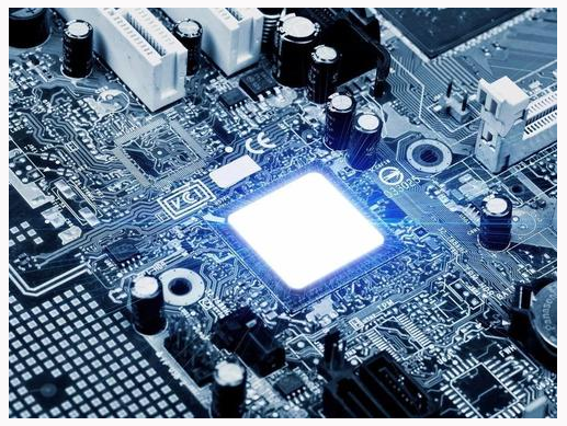
[Methods for testing common people on PCB boards]
Electrical testing usually uses a Wheatstone bridge to measure the impedance characteristics between test points to detect all continuity (ie, open circuit and short circuit). Visual testing finds defects by visually inspecting the characteristics of electronic components and the characteristics of printed circuits. Electrical testing is more accurate when looking for short-circuit or open-circuit defects. Visual testing can more easily detect incorrect gaps between conductors. Visual inspection is generally carried out in the early stages of the production process. Try to find defects and repair them to ensure The qualified rate of products.
1. Manual visual inspection of PCB board
Using a magnifying glass or a calibrated microscope, using the operator's visual inspection to determine whether the circuit board is qualified or not, and to determine when a correction operation is required, it is a traditional detection method. Its main advantages are low upfront cost and no test fixture, while its main disadvantages are human subjective error, high long-term cost, discontinuous defect detection, and difficulty in data collection. At present, due to the increase in PCB production and the shrinking of the wire spacing and component volume on the PCB, this method has become increasingly infeasible.
2. PCB board online test

Find out manufacturing defects and test analog, digital, and mixed-signal components through electrical performance testing to ensure that they meet specifications. There are several testing methods such as bed-of-needle testers and flying probe testers. The main advantages are the low test cost of each board, strong digital and functional testing capabilities, fast and thorough short-circuit and open-circuit testing, programming firmware, high defect coverage, and easy programming. The main disadvantages are the need to test fixtures, programming and debugging time, the high cost of making fixtures, and the difficulty of use.
3. PCB board function test
The functional system test is to use special test equipment in the middle stage and the end of the production line to conduct a comprehensive test on the functional modules of the circuit board to confirm the quality of the circuit board. Functional testing can be said to be an early automatic testing principle. It is based on a specific board or a specific unit and can be completed with various equipment.
There are types such as final product testing, physical model and stacked testing. Functional testing usually does not provide in-depth data such as foot-level and component-level diagnostics for process improvement, and requires specialized equipment and specially designed test procedures. It is complicated to write functional test programs, so it is not suitable for most circuit board production lines.
4. Automatic optical inspection
Also known as automatic visual inspection, it is based on optical principles and comprehensively uses multiple technologies such as image analysis, computer and automatic control to detect and deal with defects encountered in production. It is a relatively new method of confirming manufacturing defects. AOI is usually used before and after reflow and before electrical testing to improve the pass rate of electrical processing or functional testing. At this time, the cost of correcting defects is much lower than the cost after final testing, often reaching more than ten times.
5. Automatic X-ray inspection
Using the difference in the absorption rate of different substances to X-rays, see through the parts that need to be tested, and find defects. It is mainly used to detect defects such as bridging, missing pieces, poor alignment, etc. in ultra-fine pitch and ultra-high circuit boards and assembly processes. It can also use its tomographic imaging technology to detect internal defects in IC chips.
It is the current method to test the soldering quality of the ball grid array and the blocked solder balls. The main advantage is the ability to detect BGA welding quality and embedded components, without fixture cost; the main disadvantages are slow speed, high failure rate, difficulty in detecting reworked solder joints, high cost, and long program development time. This is a relatively new test. The method remains to be further studied.
6. Laser detection system
It is the development of PCB testing technology. It uses a laser beam to scan the printed board, collects all measurement data, and compares the actual measurement value with the preset qualified limit value. This technology has been proven on the bare board and is being considered for assembly board testing, and the speed is sufficient for mass production lines. Fast output, no fixtures and visual non-covered access are its main advantages; high initial cost, maintenance and use problems are its main disadvantages.
7. Size detection
Use the two-dimensional image measuring instrument to measure the hole position, length and width, position and other dimensions. Since PCB is a small, thin and soft type of product, contact measurement can easily produce deformation and cause inaccurate measurement. The two-dimensional image measuring instrument has become a high-precision size measuring instrument. After being programmed, the image measuring instrument of Sirui Measurement can realize fully automatic measurement, which not only has high measurement accuracy, but also greatly shortens the measurement time and improves the measurement efficiency.
[What are the hazards of holding the PCB board with one hand]
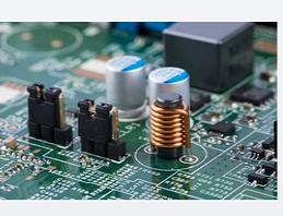
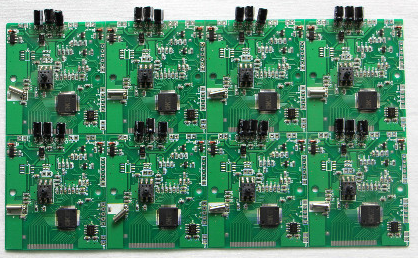
In the process of circuit board PCB assembly and soldering, smt chip processing manufacturers have many employees or customers involved in operations, such as plug-in component insertion, ICT testing, PCB splitting, manual soldering operation and installation of PCB boards Screws, installation rivets, manual crimp connectors, PCBA circulation, etc. In this series of operations, a common action is to hold the circuit board alone, which is a major factor that causes the failure of BGA and chip capacitors.
So what are the hazards of holding a PCB board with one hand?
(1) Holding the PCB board with one hand, it is generally allowed for circuit boards with small size, light weight, no BGA, and no chip capacitance; but for circuits with large size, heavy weight, and BGA and chip capacitors on the side Boards should be avoided. Because this behavior can easily cause the solder joints of BGA, chip capacitance and even chip resistor to fail. Therefore, in the process documents, the requirements for how to take the circuit board should be specified.
The easy way to hold a PCB board with one hand is the circulation process of the circuit board. Regardless of taking the board from the belt line or putting the board, most people will unconsciously adopt the practice of holding the board with one hand because it is smooth. When welding by hand, attaching heat sinks, and installing screws. Since it is necessary to complete an operation, it is natural to hold the circuit board in one hand and operate other work items in the other. These seemingly normal operations often hide great quality risks.
(2) Installing screws, in many PCBA patch processing factories, in order to save costs, tooling is omitted. When installing screws on the PCBA, the components on the back of the PCBA are often deformed due to the unevenness of the components, which can easily cause stress-sensitive solder joints to crack.
(3) Insert through-hole components
Through-hole components, especially transformers with relatively thick leads, are often difficult to accurately insert into the mounting holes due to the relatively large lead position tolerance. The operator will not think of a way to be accurate, and usually use a rigid press-in operation, which will cause bending and deformation of the PCB board, and will also cause damage to the surrounding chip capacitors, resistors, and BGAs.