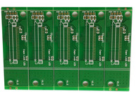
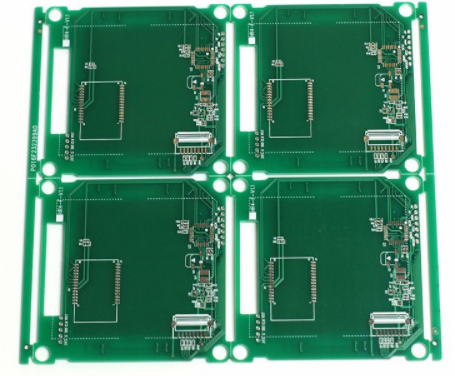
Explain and explain the PCB board design
In the following, we will explain and explain the PCB on-line test design, which is very important in PCBA processing, and I hope it will be helpful to you who are also concerned about this field.
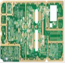
In-CirciutTest (In-CirciutTest) refers to an electrical performance test method that uses isolation technology and applies test probes to test points on the tested PCB to test the device and circuit network characteristics.
The following tests can usually be carried out:
(1 Open circuit, short circuit and connection failure of components and network connections;
(2) Missing parts, wrong parts, bad parts and plug-in errors;
(3) Carry out parameter tests on all analog devices (whether it exceeds the specification requirements);
(4) Perform functional testing on some integrated circuits (IC);
(5) Detect LSI, VLSI connection or welding failure;
(6) Detect memory or other devices with online programming errors.

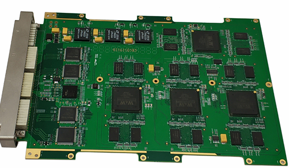
Since it is tested by the test needle bed, the design of the PCBA needs to consider the production and reliable test requirements of the test needle bed.
(1) For the PCBA for ICT testing, at least design two non-metallized holes on the diagonal of the PCB as positioning holes. The positioning aperture can specify a size by itself, such as 3.00+0.08/0mm. There is no special requirement for the distance between the positioning hole and the edge, just leave an effective distance of 1.50mm or more. It is recommended to design at a distance of 5.00mm or more from the center of the hole to the side.
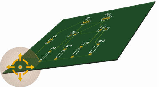
(2) The online test point refers to the contact part of the probe test. There are three main types:
1. Process pads or metallized through holes specially drawn from the circuit network;
2. Open the tin through hole of the solder mask;
3. The solder joints of through-hole plug-in devices.
(3) Requirements for the setting of test points:
1. If a node in a node network is connected to the plug-in component, then there is no need to set a test point.
2. If all components connected in a node network are boundary scan devices (ie digital devices), then this network does not need to design test points.
3. In addition to the above two cases, each wiring network should have a test point. On the single board power and ground traces, there should be at least one test point for every 2A current. The test points should be concentrated on the soldering surface as much as possible, and should be evenly distributed on the single board.
(4) Test point size requirements.
For test pads or via hole pads used for testing, the small pad diameter (referring to the outer diameter of the hole pad) should be greater than or equal to 0.90mm, and 1.00mm is recommended. The center distance between adjacent test points should be greater than or equal to 1.27mm, and 1.80mm is recommended.
(5) The small distance between the test point and the solder mask covered via is 0.20mm, and 0.30mm is recommended.
(6) The small distance between the test point and the device pad is 0.38mm, and 1.00mm is recommended.
(7) If the height of the PCB component package is less than or equal to 1.27mm, the distance between the test point and the device body should be greater than or equal to 0.38mm, 0.76mm is recommended; if the height of the component package is within the range of 1.27~6.35mm, the test point and the device The distance of the body should be greater than or equal to 0.76mm, 1.00mm is recommended; if the height of the component exceeds 6.35mm, the distance should be greater than or equal to 4.00mm, and 5.00mm is recommended.
(8) The distance between the test point and the copper foil conductor without solder mask should be 0.20mm, 0.38mm is recommended.
(9) The distance between the test point and the positioning hole should be greater than or equal to 4.50mm
How to choose the material of the PCB board
Regardless of the laminated structure of the multilayer PCB, the final product is a laminated structure of copper foil and dielectric. The materials that affect circuit performance and process performance are mainly dielectric materials. Therefore, the choice of PCB board is mainly to choose dielectric materials, including prepregs and core boards.
The choice of material mainly considers the following factors.
1) Glass transition temperature (Tg)
Tg is a characteristic property of polymers, a critical temperature that determines material properties, and a key parameter for selecting substrate materials. The PCB temperature exceeds Tg, and the thermal expansion coefficient becomes larger.
According to the Tg temperature, PCB boards are generally divided into low Tg, medium Tg and high Tg boards. In the industry, boards with a Tg around 135°C are usually classified as low-Tg boards; boards with a Tg around 150°C are classified as medium-Tg boards; and boards with a Tg around 170°C are classified as high-Tg boards.
If there are many pressing times during PCB processing (more than 1 time), or the number of PCB layers (more than 14 layers), or the soldering temperature is high (>230 degree Celsius), or the working temperature is high (more than 100 degree Celsius), or the soldering thermal stress is large (Such as wave soldering), high Tg plates should be selected.
2) Coefficient of Thermal Expansion (CTE)
The coefficient of thermal expansion is related to the reliability of welding and use. The selection principle is to be as consistent with the expansion coefficient of Cu as possible to reduce thermal deformation (dynamic deformation) during welding)
3) Heat resistance
Heat resistance mainly considers the ability to withstand the soldering temperature and the number of soldering times. Usually, the actual welding test is carried out with slightly stricter process conditions than normal welding.
It can also be selected according to performance indicators such as Td (temperature at 5% weight loss during heating), T260, and T288 (thermal cracking time).
4) Thermal conductivity
5) Dielectric constant (Dk)
6) Volume resistance, surface resistance
7) Moisture absorption
Moisture absorption will affect the PCB storage period and assembly process. Generally, the plates are easy to delamination when they are welded after absorbing moisture.