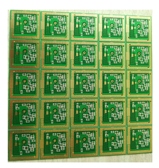
The relationship between PCB board routing length matching and frequency of difference pairs
The correct matching of trace length and frequency should take into account the whole bandwidth of the signal propagating along the trace. This has been the subject of research in differential serial protocols for the past few years, with standards such as USB4 placing specific requirements on wideband signal integrity indicators. Some sample wideband signal integrity indicators are:
Integrated differential crosstalk
Integral difference insertion loss
Integral difference return loss
Integral difference impedance deviation

By "integration", we mean that specific aspects of signal integrity apply across the relevant frequency range. In other words, if we take differential crosstalk for example, we want to reduce the differential crosstalk between two difference pairs to below a certain limit, as specified in the signaling standard. We'll see why this is important for tracking length matches in a moment.
scattered
In the time domain, we care only about the halfway transition between the two ends of the difference pair crossing the HI and LOW states (suppose binary) at the same time. Obviously, jitter poses a problem here, in that it limits your line length to a certain tolerance, so you'll never get the ends of a pair of lines to transition perfectly at the same time. In the frequency domain, we need to consider dispersion from the following sources:
Geometric dispersion: This is caused by the boundary conditions and geometry of the interconnects, which then determine how the impedance of the interconnects varies with the geometry.
Dielectric diffusion: This occurs in the PCB substrate and is independent of the geometry of the interconnect on the PCB. It includes Dk dispersion and loss.
Roughness dispersion: This additional source of dispersion occurs due to causality of the copper roughness model and skin effect at high frequencies.
Dispersion of fiber braiding: Fiber braiding in PCB laminates produces periodic dispersion changes throughout the interconnect.
Because these dispersion sources are always present in the wiring, they cause the impedance, speed,
and all other indicators of signal integrity of the actual PCB wiring to be functions of frequency. An example showing how dispersion in the real part of the Dk affects the impedance of microstrip wiring is shown below.
The speed signal
If you are familiar with transmission line theory, then you know that impedance is closely related to signal speed. Let's take the signal speed of PCB wiring as an example. The figure below shows the group and phase velocities of simulated bands with roughness and dispersion.
Group velocity and phase velocity of a sample ribbon line signal with copper roughness and dielectric dispersion.
Here we can see that the phase velocity varies greatly over a wide frequency range, up to a factor of 2 from 1MHz to 20GHz. The change in phase velocity is an important parameter here because this is the rate at which the different frequency components propagate along the interconnect. Through this change, we can see how difficult PCB trace length matching and frequency matching become for practical interconnections. We need some way to account for all frequencies, not just arbitrarily selected individual frequencies.
Broadband length matching and frequency
To develop a measure of length matching, we need to consider the allowable length deviation for a given signaling standard. We call this time deviation TLIM. We can write the following equations for length tolerances and allowable timing mismatches:
A change in length according to the allowable temporal variation.
Here, the function K is simply the propagation constant of the signal over the interconnect, which is also a function of the frequency due to dispersion. We can use statistical methods to deal with allowable length mismatches using something called the "Lp norm". Without delving too deeply into the mathematics involved, just know that this measure is equivalent to calculating the RMS difference between a function and an average that differs by only a constant. Thus, this makes it an ideal mathematical tool for addressing variations between certain target design values and signal integrity measures (impedance, impulse response attenuation/delay, crosstalk intensity, etc.).
Using the Lp norm, we can rewrite the allowable length mismatches based on some upper limits defined by tLIM for timing mismatches:
A change in length according to the allowable temporal variation.
When designing a PCB using wideband signal integrity metrics, the equation above can be considered as a constraint: when determining the size of a transmission line, this may affect the total allowable length deviation between any two lines in or between the ends of a difference pair. High speed parallel protocol. The integral is easy to calculate as long as you know the propagation constant of the transmission line. This value can then be calculated using a field solver and manually by an analysis model with standard transmission line geometry.
Just to provide some numbers for the calculation, if I use the phase velocity of the analog strip shown above, we find that the allowable length mismatch between parallel single-ended fully isolated traces is 2.07mm and the timing mismatch is 10ps if the allowable value is allowed. Note that for 10ps, this is a large portion of the edge rate of many high-speed digital signals. For the ribbon line I simulated above, this equals 1.3041 mm of allowable length mismatch