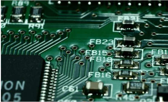
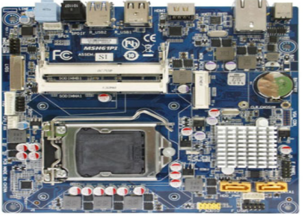
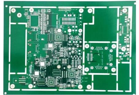
1. PCB circuit part:
1. Disconnection
A. There is a break or discontinuity on the line.
B. The length of the broken wire on the line exceeds 10mm and cannot be repaired.
C. The disconnection is near the PAD or the edge of the hole. (The open circuit can be repaired if the PAD or the edge is less than or equal to 2mm, and the open circuit is greater than 2mm from the PAD or the hole edge and cannot be repaired.)
D. Adjacent lines are disconnected side by side and cannot be repaired.
E. The line gap is broken at a turn, (the distance from the break to the turn is less than or equal to 2mm, and it can be repaired. The turn at the break is greater than 2 mm, and it cannot be repaired.)
2. PCB short circuit
A. There is a short circuit caused by foreign matter between the two wires, which can be repaired.
B. The inner short circuit cannot be repaired.
3. Line gap
A. The line gap is less than 20% of the original line width and can be repaired.
4. Line depression & indentation
A. The line is uneven, press down the line and it can be repaired.
5. Wiring tin
A. The circuit is tin-dipped (the total tin-dipped area is less than or equal to 30 square millimeters, which can be repaired, and the tin-dipped area is greater than 30 square mm, and it cannot be repaired.

6. Poor repair of the circuit
A. The offset of the compensation line or the specification of the compensation line does not meet the original line size (allowed if it does not affect the minimum width or spacing).
7, the line exposed copper
A. The solder mask on the circuit falls off and can be repaired.
8. The line is crooked
A. The distance is smaller than the original distance or there are notches, which can be repaired.
9. Line stripping
A. There has been a peeling phenomenon between the copper layer and the copper layer, which cannot be repaired.
10. Insufficient PCB line spacing
A. It is impossible to reduce the distance between the two lines by more than 30%. Repairable, more than 30% cannot be repaired.
11. Residual copper
A. The distance between the two lines cannot be reduced by more than 30%, and it can be repaired.
B. The distance between the two lines is reduced by more than 30% and cannot be repaired.
12. Line pollution and oxidation
A. Due to oxidation or contamination of the circuit, part of the circuit is discolored, darkened, and cannot be repaired.
13, the line is scratched
A. If the wire is exposed to copper due to scratches, it can be repaired. If there is no exposed copper, it will not be regarded as scratched.
14. Thin line
A. The line width is less than 20% of the specified line width and cannot be repaired.
2. PCB solder mask part:
1. Color difference (standard: upper and lower two levels)
A. The ink color of the board surface is different from the standard color. It can be compared with the color difference table to determine whether it is within the acceptable range.
2. Anti-welding cavitation
3. Anti-welding exposed copper
A. The green paint peels off the exposed copper and can be repaired.
4. Anti-welding scratches
A. If the solder mask is exposed to copper or sees the substrate due to scratches, it can be repaired.
5. Solder-resistant ON PAD
A. The parts tin pad & BGA PAD & ICT PAD are stained with ink and cannot be repaired.
6. Poor repair: the green paint coating area is too large or the repair is incomplete, the length is greater than 30mm, the area is greater than 10 square millimeters and the diameter is greater than 7 square millimeters; it is not acceptable.
7. Foreign matter
A. There are other foreign bodies in the solder mask interlayer. Repairable.
8. Uneven ink
A. There is ink accumulation or unevenness on the board surface, which affects the appearance, and local slight ink accumulation does not require maintenance.
9. VIAHOL of BGA is not plugged with ink
A. BGA requires 100% ink filling.
10. The VIA HOLE of CARD BUS is not filled with ink
A. The VIAHOLE at CARD BUS CONNECTOR needs to be 100% plugged. The inspection method is opaque under the backlight.
11. VIA HOLE is not plugged
A. VIA HOLE requires 95% cold, and the hole inspection method is opaque under backlight.
12. Tin dip: no more than 30 square millimeters
13. False exposed copper; repairable
14. Wrong ink color; not repairable
Three, through hole part
1. Hole plug.
A. Foreign matter in the part hole causes the part hole to be blocked and cannot be repaired.
2. The hole is broken.
A. The ring hole is broken and the hole cannot be connected up and down, so it cannot be repaired.
B. The dotted hole cannot be repaired.
3. Green paint in the part hole.
A. The part holes are covered by solder resist and white paint residues, which cannot be repaired.
4. NPTH, tin dip in the hole.
A. The NPTH hole is made into a PHT hole, which can be repaired.
5. Multi-hole locks can not be repaired.
6. The hole leaks the lock and cannot be repaired.
7. The hole is off, and the hole is off the PAD, which cannot be repaired.
8. The hole is big but the hole is small.
A. The large and small holes exceed the specification error value. Not repairable.
9. The VIA HOLE hole plug of BGA is not repairable.
4. PCB text part:
1. Text offset, text offset, overdraw to tin pad. Not repairable.
2. The text color does not match or the text color is printed incorrectly.
3. Text ghosting and text ghosting are still identifiable and repairable.
4. The text is missing, and the text is not repairable.
5. The text ink stains the board surface, and the text ink stains the board surface, which can be repaired.
6. The text is unclear and unclear, which affects the recognition. Repairable.
7. The text is off, there is 3M600 tape for tensile test, the text is off and can be repaired.
Five, PCB pad PAD part:
1. Tin pad gap, tin pad gap due to scratches or other factors, can be repaired.
2. There is a gap in the BGA PAD and the tin pad of the BGA part, which cannot be repaired.
3. Poor optical dots, uneven optical dots with tin-sprayed burrs, and inaccurate or inaccurate alignment caused by paint staining, causing parts to shift and cannot be repaired.
4. BGA tin spraying is uneven, the thickness of spraying tin is too thick, and the tin is flat after being pressed by external force, which cannot be repaired.
5. The optical dots fall off, and the optical dots fall off and cannot be repaired.
6. PAD falling off, PAD falling off can be repaired.
7. The QFP is not inked and cannot be repaired.
8. Less than 3 strips of QFP falling off ink and QFP falling off ink can be accepted. Otherwise it cannot be repaired.
9. Oxidation, PAD is polluted and discolored, which can be repaired.
10. PAD exposed copper, if BGA or QFP PAD exposed copper, it cannot be repaired.
11. PAD is stained with white paint or solder resist ink, and PAD is covered with white paint or ink, which can be repaired.
6. Other parts:
1. PCB sandwich separation, white spots, white spots, not repairable.
2. The weave pattern is revealed, and there are woven glass woven traces in the board, and it is not repairable if it is greater than or equal to 10 square millimeters.
3. The board surface is contaminated. There should be no dust pressure, fingerprints, oil stains, rosin, glue residue, or other external pollution on the board surface, which can be repaired.
4. The molding size is too large or too small, and the external dimension tolerance exceeds the approval standard, so it cannot be repaired.
5. Poor cutting, incomplete forming, and no repair.
6. The thickness of the board, the board is thin, and the board thickness exceeds the PCB production specifications, and cannot be repaired.
7. The height of the board warp and the board tumbler is greater than 1.6mm, which cannot be repaired.
8. Molding burrs and poor molding result in burrs and uneven board edges, which can be repaired.