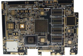
1. There must be a clearer PCB layout distinction between AC input and DC output, and the best way is to be able to isolate each other.
2. The wiring distance between the input terminal and the output terminal (including the primary and secondary DC/DC conversion) should be at least 5 mm.
3. The control circuit and the main power circuit should have a clearer layout distinction.
4. Try to avoid the parallel wiring of large current and high voltage wiring and measurement lines and control lines.
5. Put copper on the blank surface as much as possible.
6. In the high-current and high-voltage wiring connection, try to avoid using wires to connect for long distances in space. The interference it causes is difficult to deal with.
7. If the cost allows, multi-layer board wiring can be used, and there is a special auxiliary power layer and ground layer, which will greatly reduce the impact of EMC.
8. The working place is the most susceptible to interference, so try to use large-area copper wiring.
9. In the PCB design and layout, the wiring of the shielding ground cannot form an obvious loop. In this way, an antenna effect will be formed and interference will be easily introduced.

10. High-power devices are best arranged in a more regular layout to facilitate the installation of the radiator and the design of the cooling air duct.
One, ground wire design
1. Correctly choose the combination of single-point grounding and multi-point grounding.
2. Separate the digital circuit from the analog circuit
3. Make the ground wire as thick as possible
4. Form the ground wire into a closed loop
2. Electromagnetic compatibility design
1. Choose a reasonable wire width
2. Adopt the correct wiring strategy
The use of equal routing can reduce the wire inductance, but the mutual inductance and distributed capacitance between the wires increase. If the layout allows, it is best to use a grid-shaped wiring structure. The specific method is to wire one side of the printed board horizontally and the other side to wire vertically. Then connect with metallized holes at the cross holes.
In order to suppress the crosstalk between the conductors of the printed circuit board, when designing the wiring, try to avoid long-distance equal routing, and extend the distance between the wires as much as possible, and the signal wires should not cross the ground and power wires as much as possible. Setting a grounded printed line between some signal lines that are very sensitive to interference can effectively suppress crosstalk.
Three, decoupling capacitor configuration
In the DC power supply circuit, the change of the load will cause the power supply noise. For example, in digital circuits, when the circuit changes from one state to another, a large spike current will be generated on the power line, forming a transient noise voltage. Configuring decoupling capacitors can suppress noise caused by load changes, which is a common practice in the reliability design of printed circuit boards.