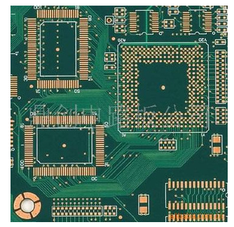
In PCB design, after completing the wiring, all you have to do is to adjust the text, individual components, wiring, and apply copper (this work should not be too early, otherwise it will affect the speed and bring trouble to the wiring), the same is for It is convenient for production, debugging and maintenance.
Copper coating usually refers to filling the blank area left by the wiring with a large area of copper foil. You can lay GND copper foil or VCC copper foil (but this way, it is easy to burn the device once a short circuit, so it is best to ground it, unless it is necessary to use it. To increase the conduction area of the power supply, to withstand a larger current before connecting to VCC). Grounding usually refers to wrapping a bunch of signal wires with special requirements with two ground wires (TRAC) to prevent them from being interfered with or interfered with by others.
1. If you use copper to replace the ground wire, you must pay attention to whether the entire ground is connected, the current size, flow direction, and whether there are special requirements to ensure that unnecessary errors are reduced.
1), check the network
Sometimes due to misoperation or negligence, the network relationship of the board drawn is different from the schematic diagram. At this time, it is necessary to check and verify. So don’t rush to hand it over to the plate maker after finishing the drawing, you should check it first, and then do the follow-up work.
2), use the simulation function

After completing these tasks, software simulation can be carried out if time permits. Especially for high-frequency digital circuits, some problems can be found in advance, which greatly reduces the amount of debugging work in the future.
2. In the PCB layout, the layout of the components on the SMT-PCB
1) When the circuit board is placed on the conveyor belt of the reflow soldering furnace, the long axis of the component should be perpendicular to the transmission direction of the device, so as to prevent the component from drifting or "tombstone" phenomenon on the board during the soldering process .
2) The components on the PCB should be evenly distributed, especially the high-power components should be dispersed to avoid local overheating on the PCB board when the circuit is working, which will cause stress and affect the reliability of the solder joints.
3) For double-sided mounting components, the larger components on both sides should be installed in a staggered position, otherwise the welding effect will be affected due to the increase of local heat capacity during the welding process.
4). PlcC/QFP and other devices with pins on four sides cannot be placed on the wave soldering surface.
5) The long axis of the large SMT device installed on the wave soldering surface should be parallel to the direction of solder wave flow, so as to reduce the solder bridging between the electrodes.
6) The large and small SMT components on the wave soldering surface should not be lined up in a straight line and should be staggered to prevent false soldering and missing soldering due to the "shadow" effect of the solder wave during soldering.