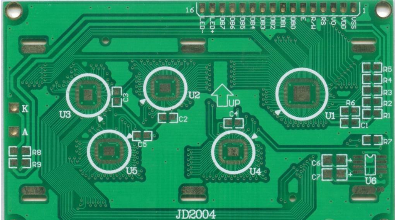
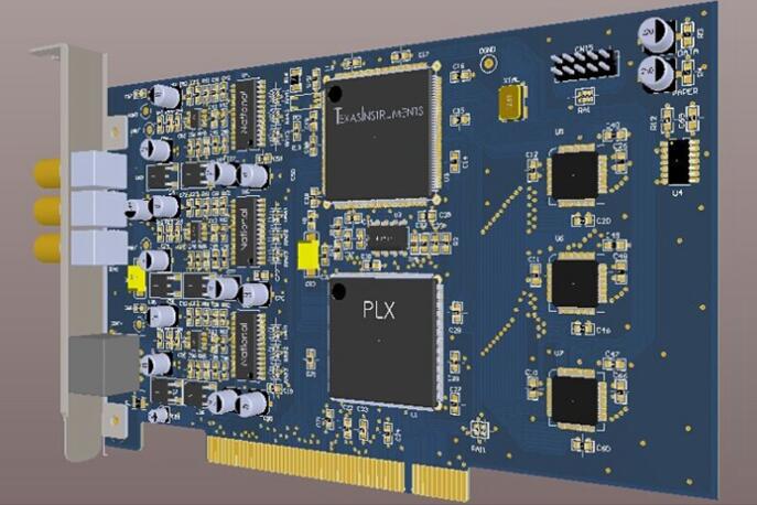
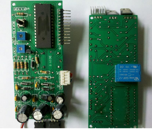
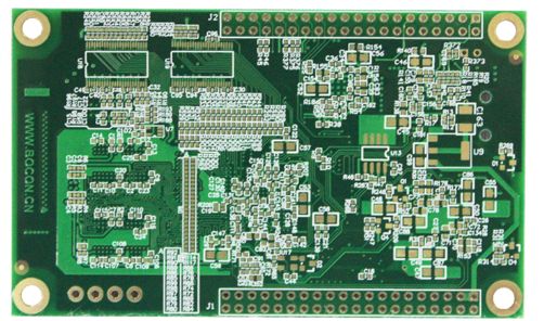
PCB proofing refers to the trial production of printed circuit boards before mass production. The main application is the process of electronic engineers designing the circuit and completing the PCB, and then conducting small batch trial production to the factory, that is, PCB proofing. The specific process of PCB proofing is as follows:
1 First, you need to inform the manufacturer of the documents, process requirements, and quantities.
Take Shenzhen Zhongqicheng PCB Factory as an example, first enter Zhongqicheng, and then register the customer number (the code please fill in "R"), and then a professional will quote for you, place an order, and follow up the production progress.
2. Cutting
1 Purpose: According to the requirements of engineering data MI, cut into small pieces to produce plates on large sheets that meet the requirements. Small sheets that meet customer requirements.
Process: large sheet - cutting board according to MI requirements - curium board - beer fillet\grinding - board out
3. Drilling
1. Purpose: According to the engineering data, drill the required aperture at the corresponding position on the sheet that meets the required size.
Process: stacked board pin - upper board - drilling - lower board - inspection\repair
4. Immersion copper
Purpose: Immersion copper is to deposit a thin layer of copper on the insulating hole wall by chemical method.
Process: rough grinding - hanging board - automatic copper sinking line - lower board - dip 1% dilute H2SO4 - thickened copper
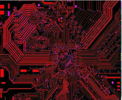
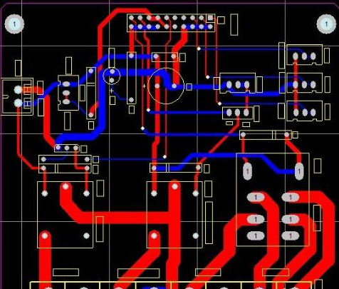
5. Graphics transfer

Purpose: Graphic transfer is to transfer the image on the production film to the board
Process: (blue oil process): grinding plate - printing the first side - drying - printing the second side - drying - exploding - developing shadow - inspection; (dry film process): hemp board - pressing film - standing - right Position-Exposure-Standing-Development-Check
6. Graphic plating
Purpose: Pattern electroplating is to electroplate a copper layer with the required thickness and a gold-nickel or tin layer with the required thickness on the bare copper skin or hole wall of the circuit pattern.
Process: upper board - degreasing - twice washing with water - micro-etching - washing with water - pickling - copper plating - washing with water - pickling - tin plating - washing with water - lower board
7. Removal of the film
Purpose: Use NaOH solution to remove the anti-electroplating coating film to expose the non-circuit copper layer.
Process: water film: insert rack - soak alkali - rinse - scrub - pass machine; dry film: release board - pass machine
8. Etching
Purpose: Etching is to use a chemical reaction method to corrode the copper layer of non-circuit parts.
9. Green oil
Purpose: Green oil is to transfer the graphic of the green oil film to the board to protect the circuit and prevent the tin on the circuit when welding parts.
Process: grinding plate-printing photosensitive green oil-curium plate-exposure-exposure; grinding plate-printing the first side-drying plate-printing the second side-drying plate
10. Characters
Purpose: Characters are provided as a mark for easy identification
Process: After the green oil finishes - cool and stand - adjust the screen - print characters - rear curium
Eleven, gold-plated fingers
Purpose: to plate a layer of nickel/gold with the required thickness on the finger of the plug to make it more hard and wear-resistant
Process: upper plate - degreasing - washing twice - micro-etching - washing twice - pickling - copper plating - washing - nickel plating - washing - gold plating
Tin plate (a process in parallel)
Purpose: Tin spraying is to spray a layer of lead tin on the exposed copper surface that is not covered with solder mask to protect the copper surface from corrosion and oxidation to ensure good soldering performance.
Process: micro-erosion - air drying - preheating - rosin coating - solder coating - hot air leveling - air cooling - washing and air drying
12. Forming
Purpose: through die stamping or CNC gong machine gong forming the shape required by the customer. Organic gong, beer board, hand gong, hand cutting
Note: The accuracy of the data gong machine board and the beer board is higher. The hand gong is second, and the minimum hand-cutting board can only make some simple shapes.
13. Test
Purpose: To pass electronic 100% testing to detect defects that affect functionality such as open circuits and short circuits that are not easy to find visually.
Process: upper mold - release board - test - pass - FQC visual inspection - unqualified - repair - return test - OK - REJ - scrap
14. Final inspection
Purpose: To pass 100% visual inspection of board appearance defects, and to repair minor defects to avoid problems and defective boards from flowing out.
Specific work flow: incoming materials - view information - visual inspection - qualified - FQA spot check - qualified - packaging - unqualified - processing - inspection OK
The above is the PCB manufacturing proofing process, I hope to help everyone.