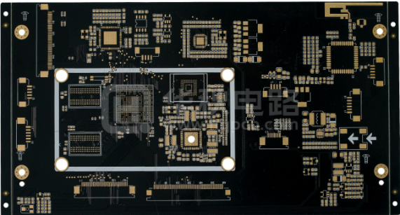
In the core structure, all conductive layers in the PCB board are coated on the core material; Shanghai SMT processing plant pointed out that in the foil structure, only the internal conductive layer of the PCB board is coated on the core material, and the outer conductive layer Layer with foil-coated dielectric board. All conductive layers are bonded together through a dielectric using a multilayer lamination process.
The nuclear material is the double-sided foil-clad board in the factory. Because each core has two sides, when fully utilized, the number of conductive layers of the PCB board is an even number. Why not use foil on one side and core structure for the rest? The main reason is: the cost of the PCB board and the bending degree of the PCB board.
Balance structure to avoid bending
The best reason not to design PCB boards with odd-numbered layers is that the odd-numbered layers PCB boards are easy to bend. When the PCB board is cooled after the multilayer circuit bonding process, the different lamination tension of the core structure and the foil-clad structure will cause the PCB board to bend.

As the thickness of the circuit board increases, the risk of bending of the composite PCB board with two different structures becomes greater. The key to eliminating PCB board bending is to adopt a balanced stack. Although the PCB board with a certain degree of bending meets the specification requirements, the subsequent processing efficiency will be reduced, resulting in an increase in cost. Because special equipment and craftsmanship are required during assembly, the accuracy of component placement is reduced, which will damage the quality.
Use even-numbered PCB
When an odd-numbered PCB board appears in the design, the following methods can be used to achieve balanced stacking, reduce PCB board production costs, and avoid PCB board bending. The following methods are arranged according to the preferred level, and the PCB chip processing factory will tell you about it:
The first point:
A signal layer and use it. This method can be used if the power layer of the design PCB is even and the signal layer is odd. The added layer does not increase the cost, but it can shorten the delivery time and improve the quality of the PCB board.
Second point:
Add an additional power layer. This method can be used if the power layer of the design PCB is odd and the signal layer is even. A simple method is to add a layer in the middle of the stack without changing other settings. First, follow the odd-numbered PCB board wiring, then copy the ground layer in the middle, and mark the remaining layers. This is the same as the electrical characteristics of a thickened layer of foil.
The third point:
Add a blank signal layer near the center of the PCB stack. This method minimizes the stacking imbalance and improves the quality of the PCB board. First, follow the odd-numbered layers to route, then add a blank signal layer, and mark the remaining layers. Used in microwave circuits and mixed media (different dielectric constants) circuits.