The correct PCB layout is one of the most important factors for a successful power supply design. The non-isolated power section is the basic building block of the power system. Understanding the direction of current flow and how the high-frequency loop is constructed is arguably the most important step in PCB design.
This article discusses power supply design techniques for the buck, boost, and single-ended primary inductance converter (SEPIC) power section.
Step-down converter
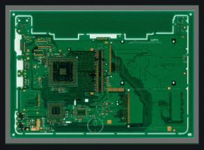
First, we use a buck converter whose output voltage is lower than the input voltage. Figure 1 shows the schematic and PCB layout of this buck converter.
This simplified schematic includes input and output capacitors, inductors, switching transistors, and blocking diodes
During the on period of the pulse width modulator (PWM), current flows along the path shown by the green arrow, from the input capacitor to the inductor through the switching transistor. During the PWM off period, current continues to flow through the inductor along the path of the pink arrow. This means that the output has a continuously flowing current.

The input high-frequency current is turned on and off once in each cycle. The most important part in this power section layout is to reduce high frequency loops. The blue arrow in the upper part reflects this loop. During the conduction of the transistor, the current flows briefly through the diode D1 to ground. During this time, if the input capacitors are not very close to each other, then this large current surge may cause some design problems.
Ensure that the power trace or power plane has enough width to carry the power current. Generally speaking, the power plane should be as large as possible except for the switch node. There is a large dV/dt signal on the switch node, which may be coupled to other parts of the PCB layout. Therefore, reducing its surface area as much as possible can achieve a good design. Use multiple vias to connect power planes on different layers. The simple rule of thumb is that each via (10mil drilling) should not exceed 1A. If you can create a continuous ground plane as large as a PCB board, it will help reduce noise and high-frequency loops.
Boost converter
The boost converter is used to generate a higher output voltage from a lower input voltage. You can use the same process in a boost converter as in a buck converter to identify critical paths and loops.
During the PWM on period, current flows from the input terminal to the switching transistor (shown by the green arrow) through the inductor. During this period, energy accumulates in the inductor, and then transfers to the output when the PWM is turned off. Now the current flows along the pink arrow, from input to output. This means that the current on the input side is continuous. The current at the output is a high-frequency switching current. In order to minimize high-frequency noise, the loop shown in blue in the figure must be as short as possible.
During the conduction period of the transistor, the current flows only briefly from the output to the ground through the diode. If this current is not properly shunted by the output capacitor, it may cause problems in the power supply design. The general layout techniques used for buck converters can also be applied to this boost converter. Minimize the switch node area and use multiple vias to connect to the ground plane.
SEPIC converter
When the input voltage is higher or lower than the output voltage, the SEPIC converter can be used. This kind of power converter can play the role of boost when the input voltage is lower than the output, and can play the role of step-down when the input voltage is higher than the output. This circuit uses two inductors or a single coupling inductor.
Because there are two inductors, there are two current paths for each part of the switching cycle. During the PWM on period, current flows along the green arrow and accumulates energy in the inductor. When the PWM is off, energy is transferred to the output through the pink current path. In this SEPIC design, the input current is continuous. The output end exhibits high-frequency switching currents, so the loop needs to be minimized. It is recommended to use a via close to the output capacitor to connect to the ground plane. The ground plane can provide a low-impedance path between all PCB components, thereby reducing noise.
Concluding remarks
Power layout design is a very tricky task. The first step is to determine how the current flows in the power supply, and then find and minimize high-frequency loops. Next, use the ground plane and the power plane to connect the PCB components in a very low impedance manner. Ensure that the plane used has enough width to carry the designed current. The high-frequency switching node should be as small as possible to reduce the chance of noise coupling to other signals. Using many vias to connect large, continuous ground planes of various devices may also be a good design.