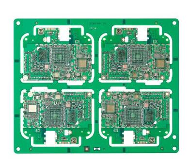
PCB patch technology is a very popular process in the electronics industry. What is a PCB? PCB is a printed circuit board and an important electronic component. It is a carrier for the interconnection of electronic components and electrical appliances. To put it simply, those electronic devices, such as computers, as small as our electronic watches, as long as there are electronic components such as integrated circuits, in order to connect the various components, they basically use the PCB board. The following is for everyone. Let's introduce the PCB board in detail.

The layers of the PCB board mainly include the power layer, the ground layer and the signal layer, and the number of layers is the sum of the number of each layer. In the design process, the first is to coordinate and classify all sources and grounds, as well as various signals, and deploy and design on the basis of classification. In general, different power supplies should be divided into different layers, and different grounds should have corresponding ground planes. Various special signals, such as high clock and frequency signals, need to be designed separately, and a ground plane needs to be added to shield the special signals to improve electromagnetic compatibility. When cost is also one of the factors to be considered, a balance should be found between the electromagnetic compatibility and cost of the system during the design process.
The first consideration in the design of the power layer is the type and quantity of the power supply. If there is only one power supply, a single power layer can be considered. In the case of high power requirements, there can also be multiple power layers to supply power to devices of different layers. If there are multiple power supplies, you can consider designing multiple power layers, or you can divide different power supplies on the same power layer. The premise of the division is that there is no crossover between power supplies. If there is a crossover, multiple power supply layers must be designed.
The design of the number of signal layers should take into account the characteristics of all signals. The layering and shielding of special signals is a problem to be considered in a limited way. Under normal circumstances, it is first to use design software to design, and then modify according to specific details. Both the signal density and the integrity of the special signal must be the issues that must be considered in the layer design. For special information, the ground plane layer must be designed as a shielding layer when necessary.
Under normal circumstances, it is not recommended to design single or double panels unless the cost is purely considered. Because the single-panel and double-panel are simple to process and cost-effective, but when the signal density is relatively high and the signal structure is more complex, such as high-speed digital circuits or analog-digital hybrid circuits, the single-panel does not have a dedicated reference ground layer, which makes the loop The area increases and the radiation increases. Due to the lack of effective shielding, the system's anti-interference ability is also reduced.
The PCB board is an important carrier in the PCB patch industry. The PCB board mainly has a power layer, a bottom layer and a signal layer. In general, different power sources must be divided into different layers, and different grounds must have corresponding ground layers, so in the design The most important thing is to layer them, and then perform operations such as deployment and design on the basis of layering.