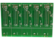
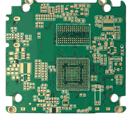
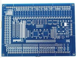
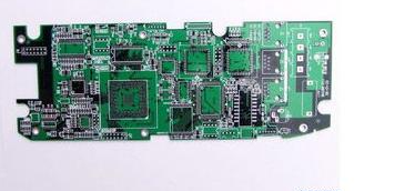
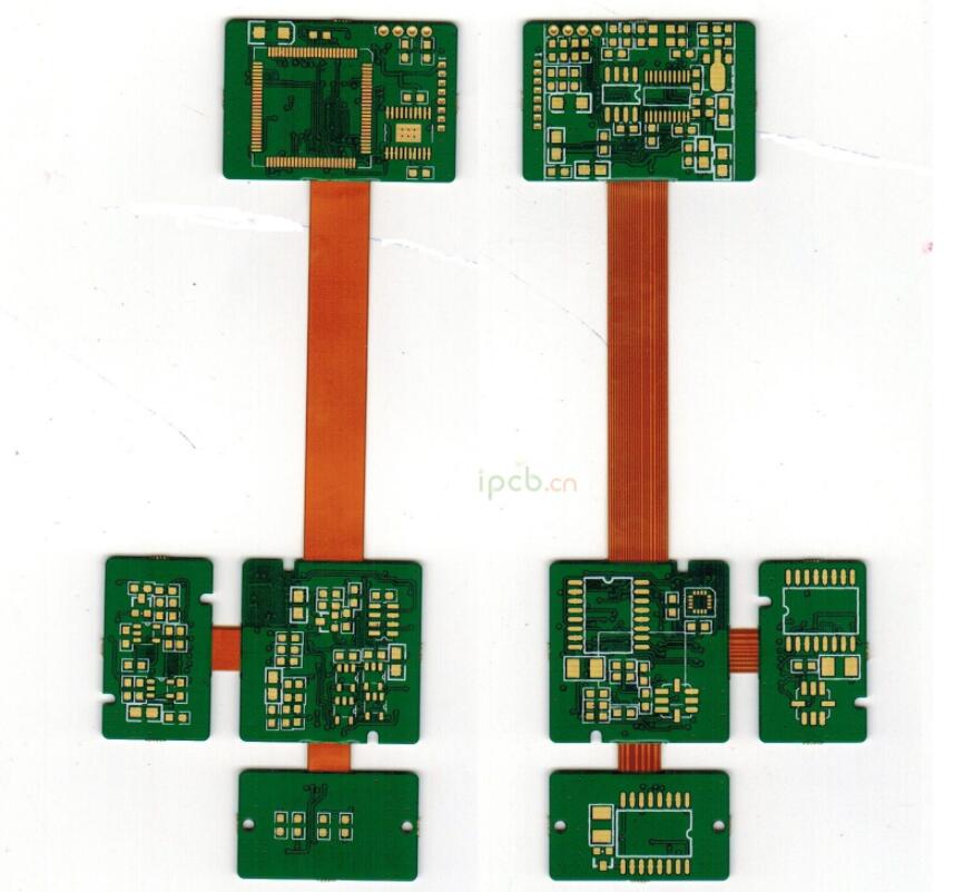
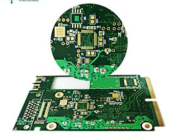
As the carrier of various components and the hub of circuit signal transmission, PCB board has become the most important and critical part of electronic information products. The quality and reliability of PCB determine the quality and reliability of the whole equipment. With the miniaturization of electronic information products and the environmental protection requirements of lead-free and halogen-free, PCBs are also developing in the direction of high density, high Tg and environmental protection. However, due to cost and technical reasons, a large number of failure problems have occurred in the production and application of PCBs, which has caused many quality disputes. In order to clarify the cause of the failure in order to find a solution to the problem and distinguish the responsibilities, it is necessary to conduct a failure analysis on the failure cases that have occurred.
Basic procedure of failure analysis
To obtain the exact cause or mechanism of PCB failure or failure, the basic principles and analysis process must be followed, otherwise valuable failure information may be missed, causing the analysis to be unable to continue or may get wrong conclusions. The general basic process is that, first, based on the failure phenomenon, the failure location and failure mode must be determined through information collection, functional testing, electrical performance testing, and simple visual inspection, that is, failure location or failure location. For simple PCB or PCBA, the failure location is easy to determine, but for more complex BGA or MCM packaged devices or substrates, the defects are not easy to observe through a microscope and are not easy to determine for a while. At this time, other means are needed to determine.

Then we must analyze the failure mechanism, that is, use various physical and chemical methods to analyze the mechanism that causes PCB failure or defect generation, such as virtual welding, pollution, mechanical damage, moisture stress, medium corrosion, fatigue damage, CAF or ion migration, Stress overload and so on. Then there is the failure cause analysis, that is, based on the failure mechanism and process analysis, to find the cause of the failure mechanism, and test verification if necessary. Generally, test verification should be performed as much as possible, and the accurate cause of induced failure can be found through test verification. This provides a targeted basis for the next improvement. Finally, according to the test data, facts and conclusions obtained in the analysis process, the failure analysis report shall be compiled. The reported facts are required to be clear, logical reasoning is strict, and organized. Do not imagine out of thin air.
In the process of analysis, pay attention to the basic principles that the analytical method should be from simple to complex, from outside to inside, never destroying the sample and then using it. Only in this way can we avoid the loss of key information and the introduction of new man-made failure mechanisms. It is like a traffic accident. If the party involved in the accident destroys or escapes the scene, it is difficult for the wise police to make an accurate determination of responsibility. At this time, the traffic laws generally require the person who fled the scene or the party who destroyed the scene to bear full responsibility. The failure analysis of PCB or PCBA is the same. If you use an electric soldering iron to repair the failed solder joints or use large scissors to forcefully cut the PCB, then there is no way to start the analysis, and the failure site has been destroyed. Especially when there are few failed samples, once the environment of the failure site is destroyed or damaged, the real failure cause cannot be obtained.
Failure Analysis Technology
Optical microscope
The optical microscope is mainly used for the appearance inspection of the PCB, looking for the failure part and related physical evidence, and preliminarily judging the failure mode of the PCB. The visual inspection mainly checks the PCB pollution, corrosion, the location of the board burst, the circuit wiring and the regularity of the failure, if it is batch or individual, is it always concentrated in a certain area, etc.
X-ray (X-ray)
For some parts that cannot be visually inspected, as well as the internal and other internal defects of PCB through holes, X-ray fluoroscopy system has to be used for inspection. X-ray fluoroscopy systems use different material thicknesses or different material densities based on different principles of moisture absorption or transmittance of X-rays for imaging. This technology is more used to check the internal defects of PCBA solder joints, the internal defects of through-holes, and the positioning of defective solder joints of BGA or CSP devices in high-density packaging.
Slice analysis
Slicing analysis is the process of obtaining the cross-sectional structure of the PCB through a series of methods and steps such as sampling, inlaying, slicing, polishing, corrosion, and observation. Through slice analysis, we can get rich information of the microstructure that reflects the quality of PCB (through holes, plating, etc.), which provides a good basis for the next quality improvement. However, this method is destructive, and once the sectioning is carried out, the sample will inevitably be destroyed.
Scanning acoustic microscope
At present, the C-mode ultrasonic scanning acoustic microscope is mainly used for electronic packaging or assembly analysis. It uses the amplitude, phase and polarity changes generated by the reflection of high-frequency ultrasonic waves on the discontinuous interface of the material to image. The scanning method is along the The Z-axis scans the information on the X-Y plane.
Micro-infrared analysis
Micro-infrared analysis is an analysis method that combines infrared spectroscopy and microscope. It uses the principle of different absorption of infrared spectra by different materials (mainly organic matter) to analyze the compound composition of the material, and combined with the microscope can make visible light and infrared light the same. The light path, as long as it is in the visible field of view, you can find the trace organic pollutants to be analyzed.
Scanning Electron Microscope Analysis (SEM)
Scanning electron microscope (SEM) is one of the most useful large-scale electron microscopy imaging systems for failure analysis. It is most commonly used for topography observation. The current scanning electron microscopes are already very powerful. Any fine structure or surface feature can be magnified. Observe and analyze hundreds of thousands of times.
Thermal analysis
Differential Scanning Calorimeter (DSC)
Differential Scanning Calorimetry (Differential Scanning Calorimetry) is a method of measuring the relationship between the power difference between the input material and the reference material and the temperature (or time) under the temperature control of the program. It is an analytical method for studying the relationship between heat and temperature. According to this relationship, the physical, chemical and thermodynamic properties of materials can be studied and analyzed. DSC has a wide range of applications, but in PCB analysis, it is mainly used to measure the curing degree and glass transition temperature of various polymer materials used on the PCB. These two parameters determine the reliability of the PCB in the subsequent process.
Thermomechanical Analyzer (TMA)
Thermal Mechanical Analysis technology is used to measure the deformation properties of solids, liquids and gels under thermal or mechanical force under program temperature control. It is a method to study the relationship between heat and mechanical properties. According to the relationship between deformation and temperature (or time), the physical, chemical and thermodynamic properties of materials can be studied and analyzed. TMA has a wide range of applications. It is mainly used for the two most critical parameters of PCB in PCB analysis: measuring its linear expansion coefficient and glass transition temperature. PCBs with substrates with too large expansion coefficients often lead to fracture failure of the metallized holes after soldering and assembly.
Thermogravimetric Analyzer (TGA)
Thermogravimetry Analysis is a method that measures the relationship between the mass of a substance and the temperature (or time) under program temperature control. In terms of PCB analysis, it is mainly used to measure the thermal stability or thermal decomposition temperature of the PCB material. If the thermal decomposition temperature of the substrate is too low, the PCB will explode or fail delamination during the high temperature of the soldering process.