Before designing a multi-layer PCB circuit board, the designer needs to determine the circuit board structure used according to the circuit scale, circuit board size, and electromagnetic compatibility (EMC) requirements. After determining the number of layers, determine the placement and how of the inner electrical layer Different signals are distributed on these layers. This is the choice of the multilayer PCB stack structure. The stack structure is an important factor affecting the EMC performance of the PCB board, and it is also an important means to suppress electromagnetic interference. Let’s learn about the PCB stack design. Point.
1. The PCB stacking method is recommended to be the Foil stacking method
2. Minimize the use of PP sheets and CORE models and types in the same stack (each layer of medium does not exceed 3 PP stacks)

3. The thickness of the PP medium between the two layers should not exceed 21MIL (thick PP medium is difficult to process, generally adding a core plate will increase the actual number of laminates and increase the processing cost)
4. PCB outer layer (Top, Bottom layer) generally uses 0.5OZ thickness copper foil, and the inner layer generally uses 1OZ thickness copper foil
Note: The copper foil thickness is generally determined according to the size of the current and the thickness of the trace. For example, the power board generally uses 2-3OZ copper foil, and the ordinary signal board generally chooses 1OZ copper foil. If the trace is thinner, 1/3QZ copper may be used. Foil to improve the yield; at the same time, avoid using core boards with inconsistent copper foil thickness on both sides of the inner layer.
5. The distribution of the PCB wiring layer and the plane layer must be symmetrical from the center line of the PCB stack (including the number of layers, the distance from the center line, the copper thickness of the wiring layer and other parameters)
Note: The PCB stacking method requires a symmetrical design. The symmetrical design refers to the thickness of the insulation layer, the type of prepreg, the thickness of the copper foil, and the pattern distribution type (large copper foil layer, circuit layer) as symmetrical to the center line of the PCB as possible.
6. The design of line width and medium thickness needs to leave sufficient margin to avoid design problems such as SI caused by insufficient margin
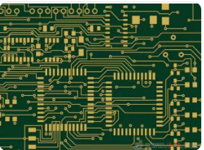
The stack of PCB is composed of power layer, ground layer and signal layer. As the name suggests, the signal layer is the wiring layer of the signal line. The power layer and the ground layer are sometimes collectively referred to as the plane layer.
In a small number of PCB designs, wiring on the power ground plane layer or power and ground network on the wiring layer is used. For this mixed type of layer design, it is collectively called the signal layer.
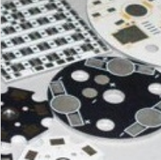
Base material and classification of printed circuit board
The choice of printed circuit board substrate should be considered in terms of electrical performance, reliability, processing technology requirements, and economic indicators. There are many substrates used for PCBs, mainly in two categories: organic and inorganic. Organic substrates are made of reinforced materials such as glass fiber cloth impregnated with resin binders, dried and covered with copper foil, and then made by high temperature and high pressure. This type of substrate is also called copper clad laminates (Copper Clad Laminations)., CCL), inorganic substrates are mainly ceramic plates and enamel coated steel substrates.
Printed circuit boards are classified into rigid printed circuit boards, flexible printed circuit boards and rigid-flexible printed circuit boards according to the rigidity and flexibility of the dielectric materials used to make the substrate. Rigid printed circuit board refers to a printed circuit board made of laminated copper foil on the surface of a substrate that is not easy to bend. It needs to be flat, has a certain mechanical strength, and can play a supporting role. Flexible printed circuit board refers to a printed circuit board made of copper foil laminated on the surface of a flexible substrate. It has good heat dissipation, ultra-thin, and can be bent, folded, wound, and can be moved and stretched arbitrarily in three-dimensional space., So it can form a three-dimensional three-dimensional circuit board. The rigid printed circuit board and the flexible printed circuit board are combined to form a rigid-flexible printed circuit board, which is mainly used for the electrical connection of the rigid printed circuit board and the flexible printed circuit board.
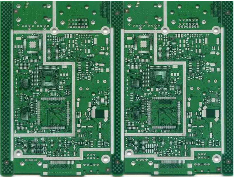
Printed circuit boards are divided into single-sided PCB boards, double-sided boards and multi-layer PCBs according to the number of layers of copper clad. Single-sided board refers to a printed circuit board on which only one surface of an insulating substrate is covered with conductive patterns. Double-sided board refers to a printed circuit board with conductive patterns on both sides of an insulating substrate, that is, the conductors on both sides of the circuit pole are connected through pads and vias. Multilayer board refers to a printed circuit board formed by alternately bonding a layer of copper foil and an insulating substrate. If it is a four-layer copper foil, it is called a four-layer board. If it is covered with copper foil on six sides, it is called a six-layer board. The electrical interconnection between the board layers is through pads, through holes, blind holes and buried holes. Wait till now. Most of the motherboards have a 4-8 layer structure, and the world's highest level can achieve nearly 100 layers.