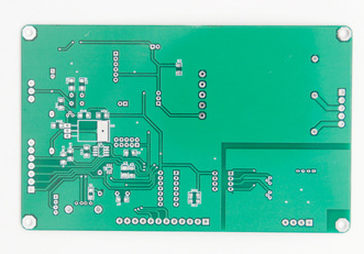
one. line
1. Minimum line width: 6mil (0.153mm). PCB circuit board production means that if the line width is less than 6mil, it will not be able to be produced. If the design conditions permit, the larger the design, the better, the larger the line width, the better the factory, the higher the yield, and the general design is usually around 10mil. This is very important, The design must be considered
2. Minimum line spacing: 6mil (0.153mm). The minimum line distance is line-to-line, and the distance from line to pad is not less than 6mil. From a production point of view, the larger the better, the general rule is 10mil. Of course, if the design is conditional, the larger the better. This is very important. Design Must consider
3. The distance between the line and the outline line is 0.508mm (20mil)
two. via via (commonly known as conductive hole)
1. Minimum aperture: 0.3mm (12mil)
2. The minimum via hole (VIA) aperture is not less than 0.3mm (12mil), the single side of the pad cannot be less than 6mil (0.153mm), and it is not limited if it is greater than 8mil (0.2mm) (see Figure 3) This point is very important, design Must consider
3. Via hole (VIA) hole-to-hole spacing (hole edge to hole edge) cannot be less than: 6mil, more than 8mil this point is very important, the design must be considered
4, the distance between the pad and the outline line is 0.508mm (20mil

5. a. Hole to line spacing:
NPTH (without welding ring): After hole compensation 0.15MM, the distance from the line is more than 0.2MM
PTH (with welding ring): after the hole compensation is 0.15MM, the distance from the line is more than 0.3MM
B. Hole to hole spacing:
PTH (with welding ring): after hole compensation 0.15mm, hole to hole above 0.45mm
NPTH hole: after hole compensation 0.15MM, hole to hole above 0.2mm
VIA: The spacing can be slightly smaller
three. PAD pad (commonly known as plug-in hole (PTH))
1. The size of the plug-in hole depends on your component, but it must be larger than your component pin. It is recommended to be larger than at least 0.2mm or above, which means that the component pin of 0.6, you must design at least 0.8 to prevent processing Tolerance makes it difficult to insert,
2, Plug-in hole (PTH) The outer ring of the pad should not be less than 0.2mm (8mil) on one side
3. Plug-in hole (PTH) The hole-to-hole spacing (hole edge to hole edge) cannot be less than: 0.3mm, of course, the larger the better (as marked in Figure 3). This is very important for circuit board production, and the design must be considered
4. The distance between the PCB pad and the outline line is 0.508mm (20mil)
Four. Solder mask
1. The plug-in hole opens the window, and the single side of the SMD window cannot be less than 0.1mm (4mil)
five. Characters (the design of the characters directly affects the production, the clarity of the characters is very relevant to the character design)
1. The character width cannot be less than 0.153mm (6mil), the character height cannot be less than 0.811mm (32mil), and the ratio of width to height is 5, that is, the character width is 0.2mm and the character height is 1mm, and so on
6: Non-metalized slotted holes The minimum spacing of the slotted holes is not less than 1.6mm, otherwise it will greatly increase the difficulty of milling
1. There are no gaps and gaps in the imposition. The gap of the gaps should not be less than 1.6 (board thickness 1.6) mm, otherwise it will greatly increase the difficulty of milling. The size of the imposition work board will vary depending on the equipment. The gap of the no-gap imposition is about 0.5mm and the process edge cannot be less than 5mm