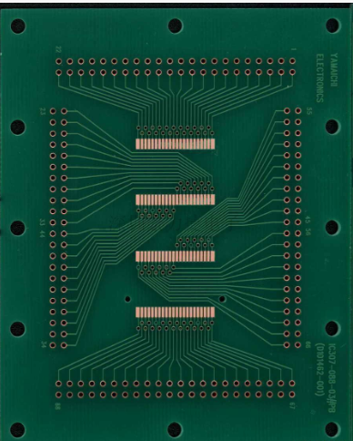
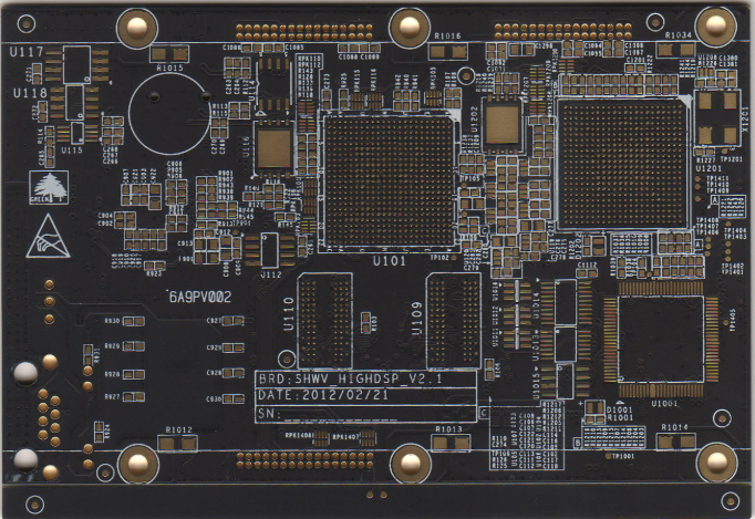
With the rapid development of electronic products, high-density, multi-function and miniaturization has become the direction of development. The components on the printed circuit board are increasing at a geometric exponential, while the size of the circuit board is constantly decreasing, and some small carrier boards are often required. If the round hole of the small carrier board is soldered to the mother circuit board with solder, due to the large volume of the round hole, there is a problem of virtual soldering, which makes the daughter and mother printed circuit boards unable to be electrically connected well, so there is a metallization half-Hole PCB. The characteristics of the metalized half-hole PCB are: the individual is relatively small, and the unit has a whole row of metalized half-holes, as the daughter board of a motherboard, through these metalized half-holes and the pins of the motherboard and components Solder together.

Difficulties in PCB processing of metallized half-hole boards:
After the metallized half-hole PCB is formed, the copper skin of the hole wall is blackened, burrs are leftover, and the position is always a problem in the forming process of various PCB factories. In particular, the entire row of semi-holes that look like stamp holes have a diameter of about 0.6mm, the hole wall spacing is 0.45mm, and the outer layer pattern spacing is 2mm. Because the spacing is very small, it is easy to short-circuit due to copper.
The general metallized half-hole PCB molding processing methods include CNC milling machine gongs, mechanical punching punching, VCUT cutting, etc. These processing methods will inevitably lead to the remaining part when removing the unnecessary part of the copper hole. There are copper wires and burrs on the section of the PTH hole, and the copper skin of the hole wall is warped and peeled off. On the other hand, when the metallized half-hole is formed, due to PCB expansion and contraction, drilling hole position accuracy, and forming accuracy, the size of the remaining half-holes on the left and right sides of the same unit varies greatly during the forming process. This is for customers to weld the assembly belt. It is very troublesome.
Traditional metallized half-hole PCB production process:
Drilling-chemical copper-full board copper-image transfer-pattern plating-film removal-etching-solder mask-surface coating half of the hole (formed simultaneously with the shape).
This metalized half hole is formed by cutting the round hole in half after the round hole is formed. It is prone to the phenomenon of half-hole copper wire residue and copper peeling, which affects the function of the half hole, resulting in a decline in product performance and yield. In order to overcome the above shortcomings, the following metallized half-hole PCB process steps should be carried out:
After the substrate is plated with copper and tinned twice, the round hole on the side of the board is cut in half to form a half hole. Because the copper layer on the hole wall is covered with a tin layer, and the copper layer on the hole wall is completely connected with the copper on the outer layer of the substrate, It involves a large binding force, which can effectively prevent the copper layer on the hole wall from being pulled off or the copper lifting up during cutting;
After the half-hole plate is formed, the film is removed and then etched. The copper surface will not be oxidized, which effectively avoids residual copper and even short circuit, and improves the yield of the metalized half-hole PCB circuit board.