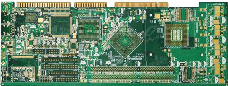
This article introduces what is the characteristic impedance in a PCB? How to solve the impedance problem.
With the upgrading of customer products, it gradually develops in the direction of intelligence, so the requirements for PCB board impedance are becoming more and more stringent, which also promotes the continuous maturity of impedance design technology. Now we summarize the impedance application and control methods for everyone to exchange and share.
What is characteristic impedance?
1. The resistance generated by alternating current in the components is related to capacitance and inductance. When there is an electronic signal waveform transmission in the conductor, the resistance it receives is called impedance.
2. Resistance is the resistance generated by direct current on the components, which is related to voltage, resistivity, and current.
Application of characteristic impedance

1. Applied to high-speed signal transmission and high-frequency circuit, the electrical performance provided by the printed board must be able to prevent reflection during signal transmission, keep the signal intact, reduce transmission loss, and play a matching role. Complete, reliable, accurate, worry-free, and noise-free transmission of signals.
2. The size of impedance cannot be simply understood as the bigger the better or the smaller the better, the key is matching.
Control parameters of characteristic impedance
The dielectric constant of the sheet, the thickness of the dielectric layer, the line width, the copper thickness, and the thickness of the solder mask.
Influence and control of solder mask
1. The thickness of PCB solder mask has little effect on impedance. When the thickness of solder mask increases by 10um, the impedance value changes only 1-2 ohms.
2. In the design, there is a big difference between the cover and no cover solder mask, single-ended 2-3 ohms, and differential 8-10 ohms.
3. In the production of impedance boards, the thickness of the solder mask is normally controlled according to the production requirements. The basic method of impedance testing is the TDR method (time domain reflectometry). The basic principle is that the instrument emits a pulse signal, which is folded back after the test piece of the PCB circuit board, and the changes in the characteristic impedance value of the emission and foldback are measured. After computer analysis, Output characteristic impedance.
Impedance problem handling
1. Regarding the control parameters of impedance, the control requirements can be achieved through mutual adjustment in production.
2. After lamination in the production, the board is sliced and analyzed. If the thickness of the medium is reduced, the line width can be reduced to meet the requirements; if the thickness is too thick, the copper can be thickened to reduce the impedance value.
3. In the test, if there is a lot of difference between the theory and the reality, the biggest possibility is that there is a problem with the engineering design and the test strip design.
The above is to what is the characteristic impedance in the PCB? How to solve the impedance problem