The technical realization method of PCB copy board is to scan the circuit board to be copied first and record the detailed position of the components. Then the components are removed to make a bill of materials (BOM), and the materials are arranged to purchase a blank board, and then scanned into a picture, processed by the copy board software and returned to the PCB board file. Then the PCB file is sent to the manufacturing board, and the purchased components are soldered to the manufactured PCB board, and the circuit board is tested and debugged.
The specific steps of PCB copy board.
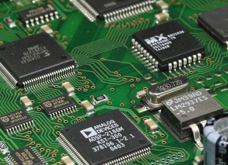
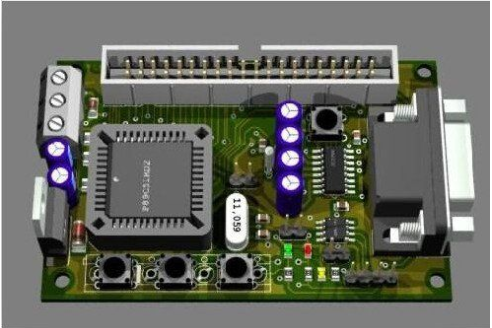
1. To obtain the PCB, first record the model parameters and positions of all vital parts, especially the direction of the diode triode. It is best to take two photos with a digital camera. Today's PCB circuit boards are becoming more and more advanced, and the diode triode is invisible at all.
2. Remove all multilayer copies of the appliance and remove tin from the PAD hole. Clean the PCB with alcohol and place it in the scanner. When scanning, you need to slightly increase the scanning pixels to obtain a clearer image. Then lightly polish the top and bottom with water gauze paper until the copper film is shiny, then put it in the scanner, start Photoshop, and scan the two layers in color. Please note that the PCB must be placed on the scanner horizontally and vertically, otherwise the scanned image will be unusable.
Adjust the contrast and darkness of the canvas so that the contrast between the copper film and the copper-free film is strong, and then convert the second picture into a black and white inspection line, if it is not clear. Then repeat this step. If you clearly store the pictures as black and white BMP format files TOP.BMP and BOT.BMP. If you find a problem with the graphics, you can also use Photoshop to repair and modify it.

4. Convert the two BMP format files to Protel format files, and convert them to the location of the two-tier pass and VIA. This shows that the first few steps are well done. If there is a deviation, please repeat the third step. Therefore, the PCB copy board is a very patient work, because a small problem will affect the quality and the matching of the copy board.
5. Convert the top BMW to the top. The PCB notices that it is yellow, and then you describe it on the top layer. And place the device according to step 2. After drawing, delete the SILK layer. Knowing to draw all the floors over and over again.
6. Transfer Toppcb and BOT.PCB to a picture in Protel.
7. Use a laser printer to print ToplayerBOTTOMLAYER to transparent film (1:1), and put the film on the PCB. Compare whether there are errors. If it is right, you will be done.
A copy like the original board was born, but only half completed. It is also necessary to test whether the electronic technical performance of the replicated board is the same as that of the original board. If so, it's over.
Note: If it is a multilayer board, carefully grind the inner layer while repeating the third to fifth steps. Of course, the naming of the graphics is determined according to the number of layers. In general, the double-sided copy board is simpler than the multi-layer copy board, and the multi-layer copy board is easier to align. Therefore, the multi-layer replica board should be particularly careful and careful, in which internal guide holes and non-guide holes are prone to problems.
Double panel copy method.
1. Scan the two BMW pictures on the bottom surface of the circuit board.
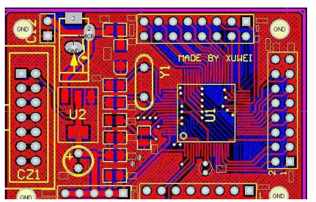
2. Open the copy board software Quickpcb2005 point file, open the base map and open the scanned picture. Use Pageup to zoom in on the screen, view the pads, and place the pads on the pads according to PP to see the line according to the PT line. Just like the pictures drawn by children. Click "Save" to generate the B2P file.
3. Open the base image and open another layer of the scanned image.
4. Click File and open the previously saved B2P file. We see that the board just copied is folded on this photo-the same PCB board hole is in the same position. It's just that the lines are different. Therefore, according to the option-floor setting, we close the top line and silk screen, leaving only the multi-level passage.
5. The top hole is in the same position as the bottom hole. Now we can draw the bottom line as we did when we were young. At this time, the B2P file has top and bottom information.
6. If the file is exported as a PCB file, a PCB file with two layers of data can be obtained, and it can be re-knitted or returned to the PCB factory for production.
Three-layer board copy method.
In fact, the four-layer board is duplicated with two double-sided boards, and the six-layer board is repeated with three double-sided boards. Multiple layers are daunting because we can't see the wiring inside. What do we think of a precision multilayer board? -Layering.
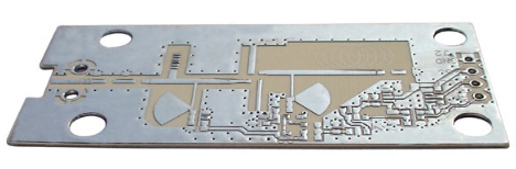
At present, there are many layering methods, such as chemical corrosion, peeling, etc., but it is easy to separate the layers and lose information. Experience tells us that sandpaper grinding is the most accurate.
When we copy the bottom of the PCB, we usually grind the surface with sandpaper to reveal the inner layer; sandpaper is ordinary sandpaper sold in hardware stores. Then press the sandpaper and rub it evenly on the PCB (if the board is small, you can hold the PCB with your fingers and rub it on the sandpaper). The key is to pave it so that it can be ground evenly.
Silk screen and green oil usually erase copper wire and copper skin. Generally speaking, a Bluetooth board can wipe a memory stick for about ten minutes in a few minutes; of course, it takes less time to do more work.
Grinding board is currently the most commonly used solution for layering, and it is also the most economical solution. We can find a discarded PCB to try. This is not a technical difficulty. It's just a bit boring. It's just a bit boring. Don't worry about that anymore.
After the PCB layout is completed, check the PCB diagram to see if the system layout is reasonable. The investigation can usually be conducted from the following aspects.
1. Whether the system layout can ensure the rationality or optimal performance of the circuit, and whether the reliability of the circuit can be guaranteed. In the layout, it is necessary to have a comprehensive understanding and planning of the direction of the signal and the power and ground wire network.
2. Whether the size of the printed board is consistent with the size of the processing drawings, which can meet the requirements of the PCB manufacturing process. It should be noted that the circuit layout and wiring of many PCB boards are designed for aesthetics and reasonableness, but the accurate positioning of the positioning plug-in is ignored. The designed circuit cannot be connected to other circuits.
3. Whether there is a conflict in two-dimensional and three-dimensional space. Pay attention to the actual size of the equipment, especially the height of the equipment. The height of welded non-layout parts generally does not exceed 3mm.
4. Whether the layout of components is densely arranged in an orderly manner. In the component layout, not only the direction of the signal and the type of the signal must be considered, but also the overall density of the device layout must be paid attention to or protected.
5. Whether the frequently replaced parts are easy to replace the plug-in board into the equipment. The convenience and reliability of regular replacement parts and plug-in should be ensured.