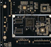
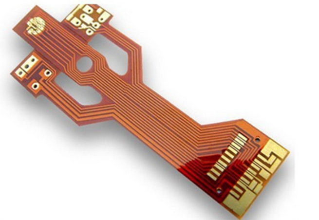
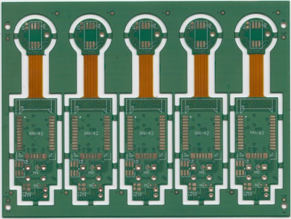
The surface process of IC Substrate's PCB gold plating must meet the requirements of both gold wire bonding and solder bonding.Because with the miniaturization and high performance of electronic equipment, semiconductor packaging circuits have added surface mount components such as BGA (Ball Grid Array). These packages use gold wire bonding to connect the semiconductor chip and the IC Substrate terminal, and the PCB and IC Substrate are connected by solder connection.
ipcb has studied the relationship between PCB gold plating on TAB (Tape Autometed Bouding) tape substrate, the thickness of the immersion gold layer and the solder joint strength. In order to meet the requirements of gold wire bonding and solder bonding, the thickness of gold plating and immersion gold must be about It is 0.2 mm. The general replacement gold plating is caused by the replacement of the base metal (nickel or nickel alloy) with gold. When the surface of the base metal is completely covered with the gold plating layer, the precipitation of gold will stop. Therefore, it is difficult to deposit a chemical with a thickness of 0.2 mm only by the general replacement gold plating method. The thickness of the gold-plated layer.

Composition and operating conditions of the PCB gold plating solution
In order to form a PCB gold-plated layer with a thickness of about 0.2 mm, roughly three basic methods are used: (1) the method of autocatalytic electroless gold plating after replacement of thin gold plating; (2) the method of using replacement-promoted gold plating to the specified thickness; 3) A method of forming a 0.2 mm ~ 0.3 mm thick electroless gold plating layer by using a substrate catalytic type electroless gold plating. However, these three gold plating solutions have various problems.
First, when autocatalytic chemical PCB gold plating is used, a reducing agent is used to reduce the precipitation of gold. As the nickel impurity concentration in the plating solution increases, the stability of the plating solution or the solder joint strength will be deteriorated or deteriorated. Wire bond strength, especially abnormal precipitation between fine lines.
Secondly, when a replacement gold plating solution is used, the solder bonding properties or wire bonding properties are also deteriorated due to oxidation or corrosion on the surface of the nickel-plated layer of the base PCB.
Finally, when the substrate-catalyzed electroless gold plating is used, the precipitation state of the gold-plated layer often depends on the composition of the substrate nickel-plated layer. In addition, cyanide-free electroless gold plating solutions are required due to environmental protection in recent years.
Based on the above problems, a cyanide-free replacement gold plating solution with sulfur-based additives was proposed, and the effect on the formation of the PCB gold plating layer was studied. The results showed that the corrosion of the PCB board nickel surface can be inhibited, and PCBs with a thickness of 0.2 mm ~ 0.3 mm can be obtained. Gold-plated layer.