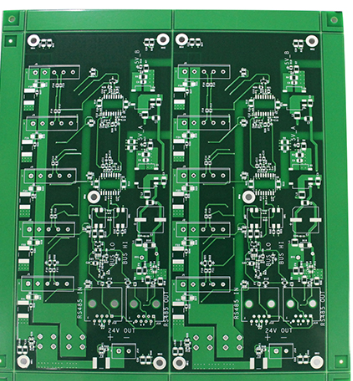
After the circuit board enters the wave soldering machine through the conveyor belt, it will pass through a certain form of flux coating device, where the flux is applied to the circuit board by wave, foaming or spraying. Since most fluxes must reach and maintain an activation temperature during soldering to ensure complete wetting of the solder joints, the circuit board must pass through a preheating zone before entering the wave trough. The Shanghai SMT chip processing plant pointed out that the preheating after the flux coating can gradually increase the temperature of the PCB and activate the flux. This process can also reduce the thermal shock generated when the assembly enters the wave crest. It can also be used to evaporate all the moisture that may be absorbed or the carrier solvent that dilutes the flux. If these things are not removed, they will boil at the peak of the wave and cause the solder to splash, or generate steam to stay in the solder to form a hollow Solder joints or blisters. In addition, due to the larger heat capacity of double-sided and multi-layer boards, they require a higher preheating temperature than single-sided boards.
At present, PCB wave soldering machines basically use thermal radiation for preheating. The most commonly used wave soldering preheating methods include forced hot air convection, electric heating plate convection, electric heating rod heating and infrared heating. Among these methods, forced hot air convection is generally considered to be the most effective heat transfer method for wave soldering machines in most processes.

After preheating, the circuit board is welded with single wave (λ wave) or double wave (spoiler wave and λ wave). For perforated components, a single wave is sufficient. When the circuit board enters the wave crest, the direction of solder flow is opposite to the traveling direction of the board, which can generate eddy currents around the component pins. This is like a kind of scrubbing, which removes all the flux and the residue of the oxide film on it, and wetting is formed when the solder joint reaches the wetting temperature.
For hybrid technology assemblies, turbulence waves are generally used in front of the lambda wave. This wave is relatively narrow and has a high vertical pressure when disturbed, which allows the solder to penetrate well between the compact pin and the surface mount component (SMD) pad, and then use the lambda wave to complete the formation of the solder joint . Before any assessment of future equipment and suppliers, it is necessary to determine all the technical specifications of the board to be soldered with wave crest, because these can determine the performance of the required machine.
Next is an introduction to identifying PCB wave soldering processes and defects
Wave soldering defect 1: Tin is too thin
Why is there such a defect? This is because there are metalized through holes that are too large or the related pads are too large during the soldering process. In addition, for the poor solderability of component pins or insufficient application of related fluxes, and when soldering, the solder temperature does not meet the standard, and the solder filling in the relevant soldering area is not solid enough or too little, etc. Such phenomena may lead to thinner defects in tin.
Wave soldering defect 2: There are bridging defects in the soldering process
Bridging defects can be said to be defects that are prone to occur in many welding processes. So how is this defect caused? Usually, bridging may be caused by changes or deterioration in the quality of the solder during soldering, or it may be because of excessive impurities or deterioration of the quality of the purchased flux. I have to say that bridging is the most common of many defects, so you should pay special attention to this type of defect when welding.
Wave soldering defect 3: Welding defects appear in the welding process
PCB virtual soldering is also a common defect problem. The cause of this defect is usually the poor solderability of the pins or solder ends of the components, or the poor solderability of the pads, and related Flux is not good at removing oxidation and so on. In addition, there may be insufficient preheating before welding, leading to the existence of related defects such as virtual welding.