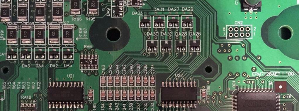
Porosity is usually a problem related to welded joints. Especially when using PCB technology to reflow solder paste, in the case of leadless ceramic chips, most of the large pores (>0.0005 inches/0.01 mm) are between the LCCC solder joints and the printed circuit board solder joints At the same time, in the fillet weld near the LCCC castle, there are only a few small pores. The existence of pores will affect the mechanical properties of the welded joint, and will damage the strength, ductility and fatigue life of the joint. This is because the growth of pores will coalesce into extensible cracks and cause fatigue. The pores will also increase the stress and covariance of the solder, which is also the cause of damage. The Shanghai SMT chip processing plant pointed out that, in addition, the solder shrinks during solidification, the delamination of exhaust gas and the entrained flux when soldering electroplated through holes are also the reasons for the porosity.
In the PCB soldering process, the mechanism of forming pores is more complicated. Generally speaking, the pores are caused by the exhaust of flux entrained in the solder in the sandwich structure during reflow (2,13) The formation of pores is mainly It is determined by the solderability of the metallized area, and changes with the decrease of flux activity, the increase of the metal load of the powder and the increase of the coverage area under the lead joint.

Reducing the size of the solder particles can only increase the porosity. In addition, the formation of pores is also related to the time allocation between the coalescence of solder powder and the elimination of fixed metal oxides. The earlier the solder paste coalesces, the more voids are formed. Generally, the proportion of large pores increases with the increase of total pores. Compared with the situation shown by the analysis results of total pores, those instructive factors that cause pores will have a greater impact on the reliability of welded joints. Some circuit board welding companies pointed out that methods to control the formation of pores include:
1. Improve the solderability of PCB components/shirt bottom;
2. Use flux with higher flux activity;
3. Reduce solder powder oxides;
4.Using an inert heating atmosphere.
5. Slow down the preheating process before reflow. Compared with the above situation, the formation of pores in BGA assembly follows a slightly different pattern. Generally speaking. In the BGA assembly using tin 63 solder blocks, the pores are mainly in Generated during the board-level assembly stage. On the pre-tinned printed circuit board, the amount of pores in the BGA connector increases with the volatility of the solvent, the metal composition and the increase in the reflow temperature, and it also increases with the decrease in the particle size. ; This can be explained by the viscosity that determines the discharge rate of the flux. According to this model, a flux medium with a higher viscosity at the reflow temperature will prevent the flux from being discharged from the molten solder. Therefore, increasing the amount of entrained flux will increase the discharge rate. The possibility of gas, resulting in a larger porosity in the BGA assembly. Without considering the solderability of the fixed metallization zone, the effect of the activity of the flux and the reflow atmosphere on the generation of pores seems to be negligible The proportion of large pores will increase with the increase of total pores, which indicates that the factors that cause pores in BGA have a greater impact on the reliability of welded joints than those shown by the analysis results of total pores. The impact is similar to the situation of the void-grown city in the SMT process.
When the solder paste is in a heated environment, the solder paste reflow is divided into five stages. First, the solvent used to achieve the required viscosity and screen printing performance begins to evaporate, and the temperature rise must be slow (about 3°C per second) to limit boiling And splashing, to prevent the formation of small tin beads. In addition, some components are more sensitive to internal stress. If the external temperature of the PCB components rises too fast, it will cause breakage.
The flux is active and the chemical cleaning action starts. The water-soluble flux and no-clean flux will have the same cleaning action, but the temperature is slightly different. Remove metal oxides and certain contaminants from the metal and solder particles to be bonded. Good metallurgical tin solder joints require "clean" surfaces
When the temperature continues to rise, the solder particles first melt individually and begin the "dark grass" process of liquefaction and surface tin absorption. This covers all possible surfaces and starts to form solder joints.
This stage is the most important. When the individual solder particles are all melted, they combine to form liquid tin. At this time, the surface tension starts to form the surface of the solder foot. If the gap between the component pin and the PCB pad exceeds 4 mil, it is most likely due to the PCB surface Tension separates the lead from the pad, which causes an open circuit at the tin point. In the cooling stage, if the cooling is fast, the tin point strength will be slightly larger, but it should not be too fast to cause temperature stress inside the component.