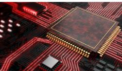
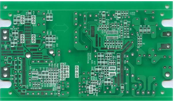
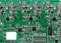
The simple statement of PCBA patch processing is that the capacitor or resistor on the electronic product is attached with a special machine, which is welded to make it stronger and not easy to fall. Just like the high-tech products such as computers and mobile phones that we often use now. Shanghai SMD processing their internal motherboards are closely arranged with tiny capacitors and resistors, and the capacitors and resistors are pasted through chip processing technology. The capacitance and resistance of high-tech patch processing is faster than manual patching, and it is not easy to make mistakes. PCBA patch processing has certain requirements for environment, humidity and temperature. At the same time, in order to ensure the quality of electronic components, the processing volume can be completed in advance. The working environment has the following requirements: temperature requirements. The best annual temperature of the workshop is 23±3 degree Celsius, and the Shanghai smt processing should not exceed the limit temperature of 15 degree Celsius~35 degree Celsius. Humidity requirements, the humidity of the patch processing workshop has a great impact on product quality.

The higher the environmental humidity, the more susceptible to damp the electronic components. The circuit board processing will affect the conductivity. At the same time, the welding is not smooth and the humidity is too low. When the workshop air is dry, static electricity will be generated. Therefore, when entering the SMT mounting processing workshop, processing Personnel also need to wear anti-static clothing. Under normal circumstances, the workshop needs to maintain a constant humidity of 45% to 70% RH.
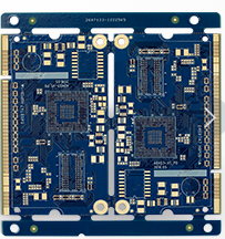
In PCBA patch processing, it is necessary to check the processed electronic products. The following is the main points of PCBA patch processing product inspection introduced by the circuit board processing factory: The component installation process quality requires that the component placement should be neat, centered, and the component type and specification should be correct; the component should be correct; there should be no missing components Stickers, wrong stickers. SMD components are not allowed to have reverse stickers. When installing a patch device with polarity requirements, the PCBA should follow the correct polarity instructions. The surface of the FPC board should have no effect on the appearance of the solder paste, foreign matter and traces. The bonding position of the components should be free of rosin or flux and foreign matter that affect the appearance and soldering tin. The bottom tin point of the component is well formed, and there is no abnormal wire drawing or tipping phenomenon.
The quality of the printing process requires that the position of the tin paste be in the middle, without obvious deviation, and the electronic processing does not affect the bonding and soldering of the tin. The printing tin paste is moderate, it can be pasted well, and there is no little tin or too much tin paste. The tin paste is formed well, should be free of tin and uneven. There should be no cracks and cuts on the bottom, surface, copper foil, wires, and through holes of the board, and there will be no short circuit due to poor cutting. The FPC board is parallel to the plane and has no convex deformation. No ambiguity, offset printing, inverted printing, offset printing, double shadow, etc. for identification information characters. The outer surface of the fpc board should not expand the bubble phenomenon. The aperture size meets the design requirements.