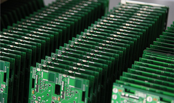
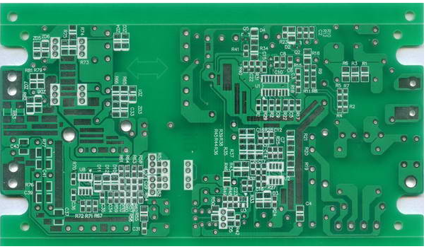
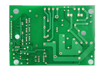
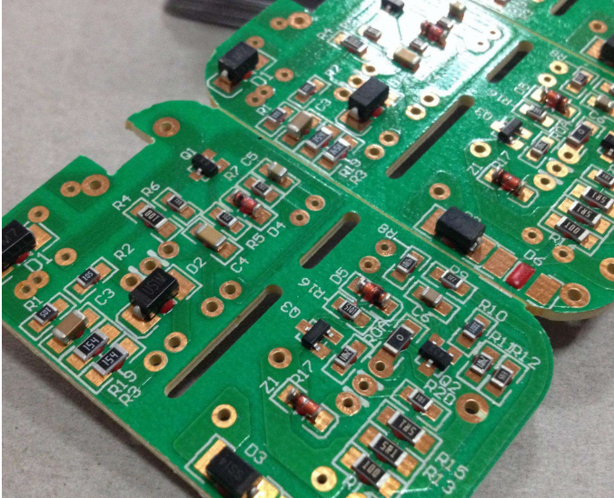
Printed circuit board manufacturing technology is a very complex and highly comprehensive processing technology. PCBA patch processing plants pointed out that, especially in the wet processing process, a large amount of water is needed, so a variety of heavy metal wastewater and organic wastewater are discharged, the composition is complicated, and the treatment is difficult. Calculate according to the utilization rate of printed circuit board copper foil of 30% to 40%, then the copper content in the waste liquid and wastewater is quite considerable. According to the calculation of 10,000 square meters of double-sided panels (the thickness of each side of the copper foil is 35 microns), the copper content in the waste liquid and wastewater is about 4,500 kg, and there are many other heavy metals and precious metals. If these metals in the waste liquid and waste water are discharged without treatment, it will not only cause waste but also pollute the environment. Therefore, the waste water treatment and the recovery of copper and other metals in the printed board production process are of great significance, and they are an indispensable part of the printed board production.
As we all know, a large amount of waste water in the production process of printed circuit boards is copper, and a very small amount is lead, tin, gold, silver, fluorine, ammonia, organics and organic complexes.

As for the processes that produce copper wastewater, there are mainly: copper sinking, full-board copper electroplating, pattern copper electroplating, etching, and various printed board pre-treatment processes (chemical pre-treatment, pre-brushing pre-treatment, pozzolan grinding board pre-treatment, etc.).
The copper-containing wastewater produced by the above process can be roughly divided into complex wastewater and non-complex wastewater according to its composition. In order to make wastewater treatment meet the national discharge standards, the maximum allowable discharge concentration of copper and its compounds is 1mg/l (calculated as copper), and different wastewater treatment methods must be adopted for different copper-containing wastewater.
Different process PCB processes-Shanghai smt chip processing factory will tell you:
One: Single-panel process
Cutting edge grinding - drilling - outer layer graphics - (full board gold plating) - etching - inspection - silk screen solder mask - (hot air leveling) - silk screen characters - shape processing - test - inspection
Two: the process flow of double-sided tin spraying board
Cutting edge grinding - drilling - heavy copper thickening - outer layer graphics - tin plating, etching tin removal - secondary drilling - inspection - screen printing solder mask - gold-plated plug - hot air leveling - silk screen characters - shape processing - testing - test
Three: Double-sided nickel-gold plating process
Cutting edge grinding - drilling - heavy copper thickening - outer layer graphics - nickel plating, gold removal and etching - secondary drilling - inspection - screen printing solder mask - screen printing characters - shape processing - testing - inspection
Four: Multi-layer board tin spraying process flow
Cutting edge grinding - drilling positioning holes - inner layer graphics - inner layer etching - inspection - blackening - lamination - drilling - heavy copper thickening - outer layer graphics - tin plating, etching tin removal - secondary drilling - inspection -Silk screen solder mask-Gold-plated plug-Hot air leveling-Silk screen characters-Shape processing-Test-Inspection
Five: Process flow of nickel-gold plating on multilayer boards
Cutting edge grinding - drilling positioning holes - inner layer graphics - inner layer etching - inspection - blackening - lamination - drilling - heavy copper thickening - outer layer graphics - gold plating, film removal and etching - secondary drilling - inspection - Screen printing solder mask-screen printing characters-shape processing-testing-inspection
Six: PCB Multilayer PCB Immersion Nickel Gold Plate Process Flow
Cutting edge grinding - drilling positioning holes - inner layer graphics - inner layer etching - inspection - blackening - lamination - drilling - heavy copper thickening - outer layer graphics - tin plating, etching tin removal - secondary drilling - inspection -Silk screen solder mask-Chemical Immersion Nickel Gold-Silk screen characters-Shape processing-Test-Inspection