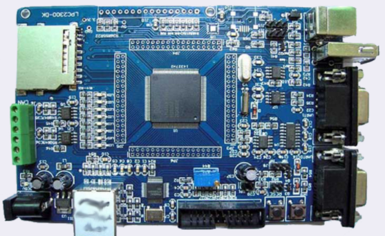
Before formulating a strategy for the test environment, preparation and understanding are key. The parameters that affect the testing strategy include:
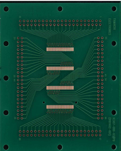
Full contact and large test pads have always been the goal of manufacturing printed circuit boards. There are usually four reasons why full access cannot be provided:
1. The circuit board size. The design is smaller; the problem is the "extra" footprint of the test board. Unfortunately, most design engineers believe that testing the accessibility of soldering on a printed circuit board (pcb) is not so important. The situation is completely different when a product has to be debugged by a design engineer due to the inability to use the simple diagnosis of the in-circuit tester (ICT). If full access is not available, the testing options will be restricted.
2. Function. The performance loss in high-speed design will affect the performance of the circuit board, but will gradually reduce the impact on product testability.
2. Board size/number of nodes. This is when the physical board size cannot be tested on any existing equipment. Fortunately, this problem can be solved by increasing the budget for new test equipment or using external test equipment. When the number of nodes is larger than the existing ICT, the problem is more difficult to solve. The DFT team must understand the testing methods so that the manufacturing department can produce good products with the least amount of time and money. Embedded self-testing, boundary scan (BS) and functional block testing can do this. The diagnosis must support the unit under test (UUT); this can only be achieved through an in-depth understanding of the test methods used, the existing test equipment and capabilities, and the fault spectrum of the manufacturing environment.

3. Failure to use, follow or understand DFT rules. Historically, DFT rules have been implemented by engineers or groups of engineers who understand the manufacturing environment, process and functional testing requirements, and component technology. In the real world, this process is lengthy and requires communication between design, computer-aided design (CAD), and testing. This kind of ubiquitous repetitive work is prone to human error and tends to act hastily under market pressure. Today, the industry has begun to use automatic "productivity analyzers" to evaluate CAD files using DFT rules. When a contract manufacturer (CM, contract manufacturer) is used, multiple sets of rules can be classified. The advantages of this method are rule continuity and error-free product evaluation.
The DFT team should be aware of the existing testing strategy. As original equipment manufacturers begin to rely on more and more CMs, the equipment used varies from plant to plant. If the manufacturer’s process is not clear, too many or too few tests may be used. Existing test methods include:
Manual or automatic visual testing, using vision and comparison to confirm the position of the component on the PCB. There are several ways to implement this technique:
one. Artificial vision is the most widely used online testing method, but due to the increase in production capacity and the shrinking of circuit boards and components, this method has become infeasible. Its main advantages are low initial cost and no test fixture. The main disadvantages are high long-term cost, discontinuous defect detection, difficult data collection, and no electrical testing and visual restrictions.
two. Automatic optical inspection (AOI) is a newer method of identifying manufacturing defects, usually used before and after reflow soldering. This is a non-electric, non-fixed online technology that uses "learn and compare" programming to minimize acceleration time. Automatic vision is better for polarity, the presence and absence of ingredients, as long as the latter's ingredients are similar to the original "learned" ingredients. Its main advantages are easy tracking and diagnosis, fast and easy program development, and no fixtures. The main disadvantages are poor short-circuit recognition ability, high failure rate, and no electrical test.
three. Automatic X-ray inspection (AXI) is currently the only method used to inspect the quality of ball grid arrays (BGA) and occluded solder balls. It is a non-electrical, non-contact technology that can find defects in the early process and reduce the work in process (WIP). Progress in this area includes pass/fail data and component-level diagnostics. There are currently two main AXI methods: two-dimensional (2d), looking at the complete board, and three-dimensional (3d), shooting multiple images at different angles. Its main advantage is the unique BGA welding quality and embedded parts inspection tools, no fixture cost. The main disadvantages are slow speed, high failure rate, difficult rework solder joint inspection, high single board cost, and long program development time.
Four. The manufacturing defect analyzer (MDA) is a good tool for high-volume/low-mix environments, where testing is only used to diagnose manufacturing defects. When the residual reduction technology is not used, repeatability between testers is an issue. In addition, MDA does not have a digital driver, so it is impossible to perform functional tests on the components or firmware on the programming board. The test time is shorter than the visual inspection time, and MDA can catch up with the beat speed of the production line. This method uses a needle bed, so the output can be diagnosed.
Its main advantages are lower initial cost, lower work-in-process cost, lower programming and program maintenance cost, higher output, easy follow-up diagnosis, and fast full short and open circuit testing. The main disadvantages are the inability to confirm whether the bill of materials (BOM) conforms to the unit under test (UUT), no digital confirmation, no functional test capability, no firmware call, and usually no test coverage indication., Board and board line-to-line repeatability, fixture cost and usage issues.
five. In recent years, due to the improvement of mechanical precision, speed and reliability, flying probe testers have been widely used. In addition, the market's requirements for fast switching, prototyping and low-volume manufacturing require no fixture test systems, making flying probe testing an ideal test choice. The best probe solution provides learning capabilities and BOM testing, which will automatically increase monitoring during the testing process. Probe software should provide an easy way to load CAD data, because X-Y and BOM data must be used in the programming process. Since the accessibility of the nodes on one side of the single board may be incomplete, the test generation software should automatically generate a non-repetitive split program.
The probe uses vectorless technology to test the connection of digital, analog, and mixed-signal components; this should be done through capacitive plates, and the user can use capacitive plates on both sides of the UUT.
The main advantages of the flying probe tester are that it is the fastest time-to-market tool, automatic test generation, no fixture cost, good diagnosis and easy programming. The main disadvantages are low output, limited digital coverage, fixed asset costs and usage issues.
6. Functional testing can be said to be the earliest automatic testing principle, and its importance has been renewed. It is a specific board or specific unit, which can be completed with a variety of equipment. To give a few examples:
Final product testing is the most common method of functional testing. The cost of testing the final unit after assembly is high, which reduces operating errors. However, diagnosis is non-existent or difficult, which adds to the cost. Only by testing the final product, if the automated testing does not provide software or hardware protection, there is a chance of damage to the product. The final product test is also very slow and usually takes up a lot of space. When the standard must be met, this method is usually not used because it usually does not support parameter measurement.
The main advantages of final product testing are the lowest initial cost, one-time assembly, product and quality assurance. Its main disadvantages are low diagnostic resolution, slow speed, high long-term cost, FPY, circuit board or machine damage due to no short-circuit detection, high maintenance cost, and no parameter detection capability.
The latest thermal models are usually placed in different stages of assembly, not just in the final test. In terms of diagnosis, it is better than the final product test, but because it needs to set up a special test unit, the cost is higher. If the program debugging only tests a specific board, then the physical model may be faster than the final product test. Unfortunately, due to lack of protection, the test bench may be damaged if a short circuit is not diagnosed in the previous process.
Its main advantage is the low initial cost. The main disadvantages are low space efficiency, high maintenance cost of test equipment, short-circuit damage of the test unit, and no parameter test capability.
Non-contact testing methods such as lasers are the latest developments in PCB testing technology. This technology has been verified in the field of bare boards, and tests on filler boards are being considered. This technology only uses line of sight, unshielded access to detect defects. Each test is at least 10 milliseconds, which is fast enough for a large-scale production line.
Its main advantages are fast production, no need for fixed equipment, sight/non-coverage channels; the main disadvantages are low test efficiency, high initial cost, and many maintenance and use problems.