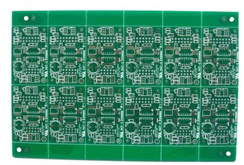
Multilayer PCB board is a kind of special printed circuit board, its existence "place" is generally special, for example: PCB multi-layer board will exist in the circuit board. This kind of multilayer board can help the machine conduct various circuits. Not only that, but it can also have an insulating effect, and it will not allow electricity to collide with each other, which is absolutely safe. Want to get a better performance multi-layer PCB board, you need to design carefully, and then I will explain how to design a PCB multi-layer board.
1. Determination of board shape, size and number of layers
▪ Any printed board has the problem of cooperating with other structural parts. Therefore, the shape and size of the printed board must be based on the product structure. However, from the perspective of the production process, it should be as simple as possible, generally a rectangle with a not too wide aspect ratio to facilitate assembly, improve production efficiency, and reduce labor costs.
▪ The number of layers must be determined according to the requirements of circuit performance, board size and circuit density. For multilayer printed boards, four-layer and six-layer boards are the most widely used. Taking four-layer boards as an example, there are two conductor layers (component surface and soldering surface), a power layer and a ground layer.
▪ The layers of the multi-layer board should be symmetrical, and it is best to have an even number of copper layers, that is, four, six, eight, etc. Because of the asymmetrical lamination, the board surface is prone to warping, especially for surface-mounted multilayer boards, which should be paid more attention.

2. The location and orientation of the components
▪ The location and placement direction of components should first be considered in terms of circuit principles and cater to the direction of the circuit. Whether the placement is reasonable or not will directly affect the performance of the printed board, especially for high-frequency analog circuits. Obviously, the location and placement requirements of the device are more stringent.
▪ Reasonable placement of components, in a sense, has predicted the success of the printed board design. Therefore, when starting to lay out the layout of the printed board and determine the overall layout, a detailed analysis of the circuit principle should be carried out, and the location of special components (such as large-scale ICs, high-power tubes, signal sources, etc.) should be determined first, and then Arrange other components and try to avoid factors that may cause interference.
▪ On the other hand, it should be considered from the overall structure of the printed board to avoid uneven and disordered arrangement of components. This not only affects the beauty of the printed board, but also brings a lot of inconvenience to assembly and maintenance work.
How do electronic hardware engineers design multi-layer PCB boards
The function of PCB board
In electronic equipment, the printed circuit board usually plays four roles.
(1) Provide necessary mechanical support for various components in the circuit.
(2) Provide electrical connections for circuits to achieve wiring or electrical insulation between various components such as integrated circuits.
(3) Provide the electrical characteristics required by the circuit, such as characteristic impedance.
(4) Mark the various components installed on the board with marking symbols for easy insertion, inspection and debugging.
Hardware engineer’s electronic product design process: project initiation, market research, project planning, project detailed design, schematic design, PCB layout, wiring, PCB board manufacturing, soldering, function, performance testing and other links. During the design process, generally follow the steps below The steps for electronic product design steps:
Step 1: Obtain the functions that the product needs to implement;
Step 2: Determine the design plan and list the required components;
Step 3: According to the component list, draw the component symbol library;
The fourth step: According to the function to be designed, call the component symbol library, draw the schematic diagram, and simulate with the simulation software;
Step 5: Draw the component package library according to the actual component shape;
Step 6: According to the schematic diagram, call the component package library and draw the PCB diagram;
The seventh step: PCB proofing production;
The eighth step: circuit welding, debugging, measurement and testing, etc. If it does not meet the design requirements, repeat the above steps.
In the above electronic product design process, PCB design is the most important link, and it is also the core technology of electronic product design. In the actual circuit design, after the schematic drawing and circuit simulation are completed, the actual components in the circuit need to be finally mounted on a printed circuit board (PCB). The drawing of the schematic diagram solves the logical connection of the circuit, and the physical connection of the circuit components is realized by the copper foil on the PCB.