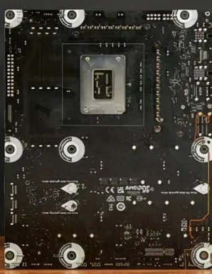
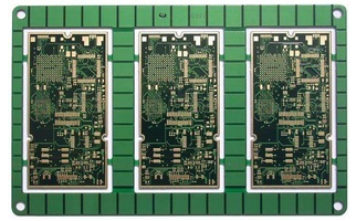
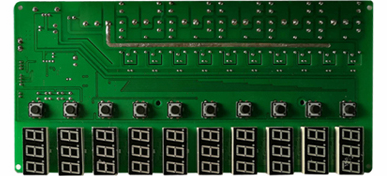
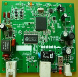
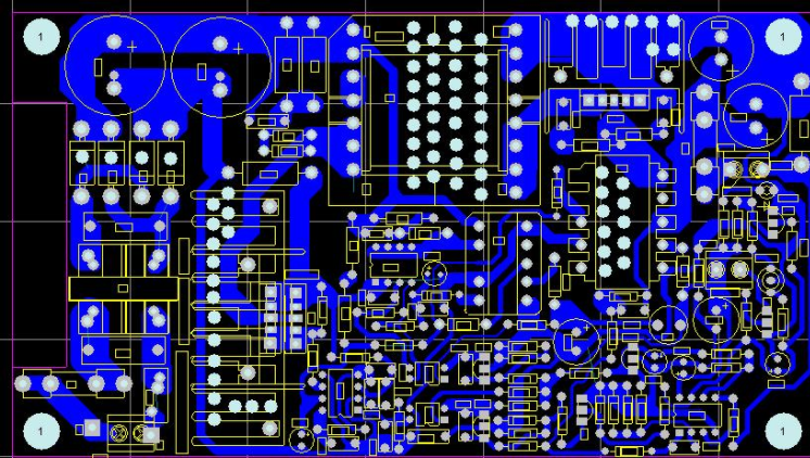
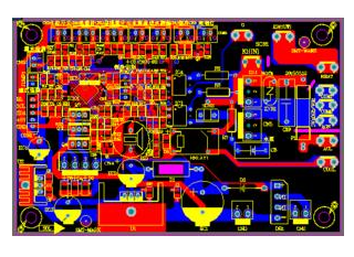
PCB
PCB is the base material of the product as a whole, and the PCB quality directly affects the welding quality and the scope of application and life of the product. The following
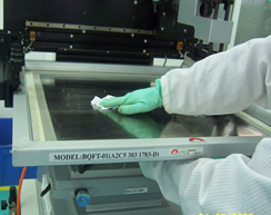
We introduce the pre-welding inspection of PCB by using tools such as visual inspection coordination and calipers for the five aspects of PCB warpage and distortion, solderability, appearance, golden fingers and special materials. There is a prerequisite that needs to be emphasized, as long as it is related to SMT materials, you need to wear anti-static gloves and wrist straps, so as not to damage the device or pollute the PCB.
1. Warpage and distortion
There are many reasons for the warpage and distortion of the PCB. The reasons other than the design may be due to the humidity of the storage environment or the placement position that cannot meet the horizontal requirements. According to the regulations, the acceptable range should be controlled at 0.5% of the diagonal length of the PCB board. the following,
Of course, there should be room for fluctuations in this range for the complexity of the board. For example, the number of large BGAs on the PCB is large, and the integration is high, and the warpage of the board should be controlled more strictly. Similarly, if there are only some small chips and resistors on the PCB If the degree of integration is low, the range can be appropriately relaxed. At present, the degree of warpage permitted by various electronic assembly plants, regardless of double-sided or multi-layered,

The thickness of 1.6mm is usually 0.70 ~ 0.75%. For many SMT and BGA boards, the requirement is 0.5%.
Some electronics factories are urging to increase the standard of warpage to 0.3%. The method of testing warpage is in accordance with GB4677.5-84 or IPC-TM-650.2.4.22B. Put the printed board on the verified platform, insert the test pin to the place where the degree of warpage is the greatest, and divide the diameter of the test pin by the length of the curved edge of the printed board to calculate the warpage of the printed board. song
Degree.
2. Solderability
PCB pads are easily oxidized when exposed to the air for a long time. If the pads are oxidized and continue to be soldered, a series of problems such as poor pad wetting and virtual soldering will result. Therefore, the solderability of the PCB must be tested before soldering. The inspection method generally adopts visual inspection. For suspected PCB, the edge immersion test is carried out [Note 1]. Visual inspection can directly pay attention to the brightness of the pad,
Generally, tinned pads or gold-plated pads appear darker after being oxidized; if you are in doubt, you can wipe a certain part with an eraser. Compared with the previous one, it is also a simple method to detect PCB oxidation.
PCB also has special pads of water-gold board. The color of water-gold board is much lighter than that of normal gold-plated board. The electroplating layer of this pad is very thin. The thinnest part of the Au layer is only 0.05um. The Ni layer is easy to oxidize. Very poor weldability, leading to welding defects
When many processing plants encounter this kind of PCB, the incoming inspection must be carried out before the placement, and cannot be exposed to the air for a long time. The placement is performed immediately after opening the vacuum package, otherwise the principle of no placement and no soldering is adhered to.
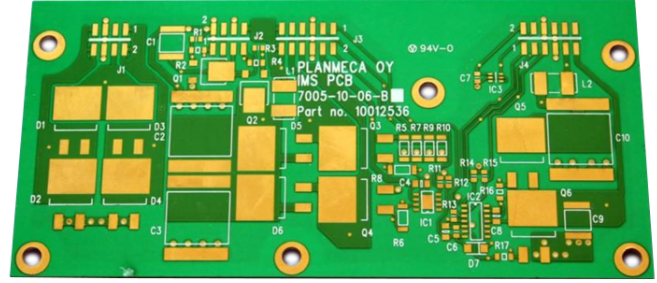
3. Appearance
The appearance of the PCB is very important to customers who directly sell finished PCBs. Of course, it may also directly affect the function of the product. Therefore, the damage of the appearance can be considered in the following two situations by simple visual inspection:
1), only affect the appearance without affecting the use of the board
1. Knock, 2. Halo
3. Friction damage4. Scratches (no damage to the solder mask and no obvious depth)
5. Exposed copper (no obvious depth, to ensure that there is no damage to the wire, you can repair the solder mask)
In the above five situations, if the customer does not sell the light board or has special requirements for appearance, they can continue to use it without affecting the performance of the product itself. However, if the customer directly sells the finished product, the above situation is unacceptable.
2) The change in appearance may cause damage to the PCB as a whole
1. Bubbling/delamination (will affect the internal circuit of PCB)
2. Scratches (broken ring solder mask, there is a certain depth, which may cause cutting to the PCB circuit)
If you encounter these two unrepairable problems, you can directly request to replace the PCB, because the consequences of these two situations are unknown.
Can be used blindly.
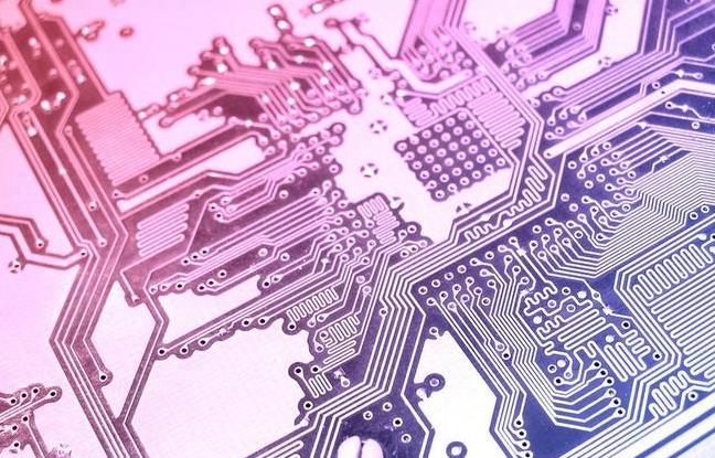
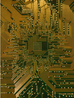
4. Gold finger
Golden finger is also special for PCB. It is the electrical pin that connects PCB to other devices such as motherboard and chassis. Therefore, its quality is very important for the entire product, so the incoming inspection must be relatively strict. General inspection needs Pay attention to several aspects:
1) There are scratches or pits in the middle 3/5 area of the gold fingers, which are mainly manifested in the deep wound, resulting in copper leakage, the recessed area exceeds 6 mil, or more than 30% of the pressure on the entire row of gold fingers. 2) Gold Finger oxidation, mainly reflected in the darkening or reddening of the color;
3) The plating layer is peeled off, and the plating layer shall be peeled or lifted after a tear test;
4) Gold finger pollution, gold finger
Tin, paint, glue or other contaminants;
5) The golden finger is not beveled or the length of the beveled edge is poor
6) The golden fingers have poor cutting edges, which are manifested in the protruding glass bundles, missing corners, not straight cutting edges, and hairs. If you have any of the above problems, you need to promptly report back to the customer and request to replace the PCB.
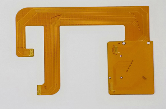
5. Special circumstances
FPC flexible board, this kind of PCB is not very common in production, but it has the characteristics of high wiring density, light weight and thin thickness.
In particular, this kind of PCB is involved in many fields. It is made of polyimide or polyester film.
Highly reliable flexible printed circuit board, according to its characteristics, we cannot leave it untreated during reflow soldering
The PCB is directly soldered, otherwise the PCB blistering (delamination) will occur. Therefore, the FPC board needs to be passed through before soldering.
Drying for more than 4 hours will reduce the occurrence of problems such as poor soldering and PCB damage.
5. PCB empty board test
Some customers require that the incoming PCB be tested, the most common is the short circuit test, that is, the large chip, BGA
The surrounding capacitance is tested, the test method is very simple, just use the multimeter buzzer file to test; if there are special customers
It is also required to conduct live test on the empty board. Of course, the test tool is also a multimeter. At this time, the customer is required to provide the corresponding
Should test points, and test required values, etc.