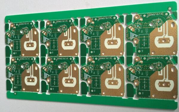
1. Film production management and inspection
Constant temperature and humidity room (21 ± 2°C, 55 ± 5%), dustproof; line width process compensation.

2, jigsaw design
The edge of the jigsaw panel should not be too narrow, the plating layer is uniform, and the plating is added with false cathodes to disperse the current;
Design the coupon for the Z0 edge test on the jigsaw board.
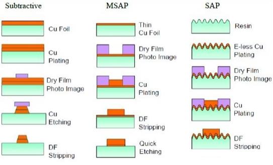
3, etching
Strict process parameters, reduce side corrosion, and conduct first inspection;
Reduce the residual copper, copper slag and copper scrap at the edge of the wire;
Check the line width and control it within the required range (± 10% or ± 0.02mm).
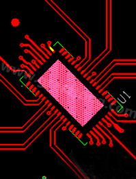
4, AOI inspection
The inner layer board must find the wire gaps and protrusions. For the 2GHZ high-speed signal, even the 0.05mm gap must be scrapped; controlling the inner layer line width and defects is the key.
5, lamination
Vacuum laminator, reduce the pressure to reduce the flow of glue, try to keep the amount of resin as much as possible, because the resin affects the εr, the resin is stored more, and the εr will be lower. Control the tolerance of laminate thickness. Because the thickness of the plate is not uniform, it indicates that the thickness of the medium changes, which will affect Z0.
6. Choose a good base material
Strictly cut the material according to the plate model required by the customer. The model is wrong, the εr is wrong, the board thickness is wrong, the PCB manufacturing process is all right, and the same is scrapped. Because Z0 is greatly affected by εr.
7, solder mask
The solder mask on the board surface will reduce the Z0 value of the signal line by 1 to 3Ω. Theoretically, the solder mask thickness should not be too thick, but in fact the effect is not great. The surface of the copper wire is in contact with air (εr = 1), so the measured value of Z0 is higher. However, the Z0 value measured after the solder mask will drop by 1 to 3 Ω. The reason is that the εr of the solder mask is 4.0, which is much higher than that of air.
8. Water absorption
The finished multilayer PCB board should avoid water absorption as much as possible, because the water εr = 75, which will bring a great drop and unstable effect to Z0.
The above is the introduction to the characteristic impedance control printed board process control, Ipcb is also provided to PCB manufacturers and PCB manufacturing technology