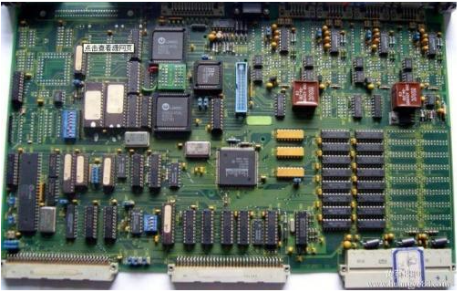
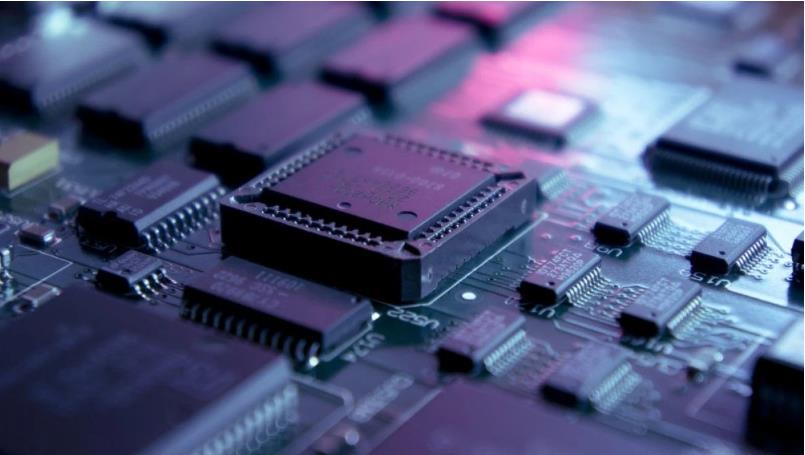
For PCB surface mount boards, especially the mounting of BGA and IC, the via hole plug must be flat, convex and concave plus or minus 1mil, and there must be no red tin on the edge of the via hole; the via hole hides the tin ball, in order to achieve According to customer requirements, the via hole plugging process can be described as diverse, the process is particularly long, the process is difficult to control, and often there are problems such as oil drop during hot air leveling and green oil solder resistance experiments; oil explosion after curing. According to the actual conditions of production, we summarize the various plugging processes of PCB, and make some comparisons and explanations in the process and advantages and disadvantages: (Note: The working principle of hot air leveling is to use hot air to make the surface of the printed circuit board and the excess inside the hole The solder is removed, and the remaining solder is evenly coated on the pads, non-solder resist lines and surface packaging points, which is one of the surface treatment methods of printed circuit boards.)
1. Hole plugging process after hot air leveling
The process flow is: board surface solder mask--HAL--plug hole--curing. Non-plugging process is adopted for production. After hot air leveling, aluminum sheet screen or ink blocking screen is used to complete the via hole plugging required by customers for all fortresses. The plug hole ink can be photosensitive ink or thermosetting ink.
In the case of ensuring the same color of the wet film, the plug hole ink is best to use the same ink as the board surface. This process can ensure that the through holes will not lose oil after the hot air is leveled, but it is easy to cause the plugging ink to contaminate the board surface and uneven. Customers are prone to false soldering (especially in BGA) during mounting. So many customers do not accept this method.

2. Hot air leveling and plug hole technology
2.1 Use aluminum sheet to plug the hole, solidify, and polish the board to transfer the graphics
This technological process uses a numerical control drilling machine to drill out the aluminum sheet that needs to be plugged to make a screen, and plug the holes to ensure that the via hole plugging is full. The plug hole ink can also be used with thermosetting ink. Its characteristics must be high in hardness., The shrinkage of resin is small, and the bonding force with the hole wall is good. The process flow is: pre-treatment -- plug hole -- grinding plate -- pattern transfer -- etching -- board surface solder mask
This method can ensure that the plug hole of the via hole is flat, and there will be no quality problems such as oil explosion and oil drop on the edge of the hole when leveling with hot air. However, this process requires one-time thickening of copper to make the copper thickness of the hole wall meet the customer's standard. Therefore, the requirements for copper plating on the entire board are very high, and the performance of the plate grinding machine is also very high, to ensure that the resin on the copper surface is completely removed, and the copper surface is clean and not polluted. Many PCB factory do not have a one-time thickening copper process, and the performance of the equipment does not meet the requirements, resulting in not much use of this process in PCB factory.
2.2 After plugging the hole with aluminum sheet, directly screen-print the board surface solder mask
In this process, a CNC drilling machine is used to drill the aluminum sheet that needs to be plugged to make a screen, which is installed on the screen printing machine for plugging. After the plugging is completed, it should not be parked for more than 30 minutes. The process flow is: pre-treatment-plug hole-silk screen-pre-baking-exposure one by one development-curing
This process can ensure that the via hole is well covered with oil, the plug hole is flat, and the color of the wet film is consistent. After the hot air is leveled, it can ensure that the via hole is not tinned and the tin bead is not hidden in the hole, but it is easy to cause the ink in the hole after curing. The soldering pads cause poor solderability; after the hot air is leveled, the edges of the vias bubble and lose oil. It is difficult to use this process to control production, and it is necessary for process engineers to use special processes and parameters to ensure the quality of the plug holes.
2.3 The aluminum sheet is plugged into the hole, developed, pre-cured, and polished, and then solder resist is performed on the surface of the board.
Use a CNC drilling machine to drill out the aluminum sheet that requires plugging holes to make a screen, install it on the shift screen printing machine for plugging holes. The plugging holes must be full and protruding on both sides. The process flow is: pre-treatment-plug hole-pre-baking-development-pre-curing-board surface solder mask
Because this process adopts plug hole curing to ensure that the via hole does not lose oil or explode after HAL, but after HAL, it is difficult to completely solve the problem of tin beads in the via hole and tin on the via hole, so many customers do not accept it.
2.4 PCB board surface solder mask and plug hole are completed at the same time.
This method uses a 36T (43T) screen, installed on the screen printing machine, using a pad or a bed of nails, and when completing the board surface, all the through holes are plugged. The process flow is: pretreatment-screen printing- -Pre-baking-exposure-development-curing.
The process time is short and the equipment utilization rate is high. It can ensure that the via holes will not lose oil after the hot air leveling, and the via holes will not be tinned. However, due to the use of silk screen for plugging the holes, there is a large amount of air in the via holes., The air expands and breaks through the solder mask, resulting in cavities and unevenness. There will be a small amount of through holes hidden in the hot air leveling. At present, after a lot of experiments, choosing different types of inks and viscosity, adjusting the pressure of the screen printing, etc., have basically solved the hole and unevenness of the vias, and this process has been used to mass produce PCBs.