In the PCB circuit board processing, when the surface tension of the solder is destroyed, it will cause poor soldering of surface mount components. The main manifestation of poor wetting is that during the soldering process, there is no reaction between the substrate solder area and the metal after the solder is infiltrated, resulting in less soldering or missing soldering.
The main causes of poor wetting are:
1. The surface of the welding area is contaminated, the surface of the welding area is stained with flux, or metal compounds are generated on the surface of the SMD component. Will cause poor wetting. Such as sulfide on the surface of silver and oxide on the surface of tin will cause poor wetting.
2. When the residual metal in the solder exceeds 0.005%, the flux activity will decrease and poor wetting will also occur.
3. During wave soldering, there is gas on the surface of the substrate, which is also prone to poor wetting.
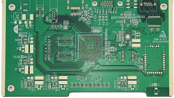
Single-sided circuit board processing four-layer immersion gold medical board finished product
The methods to solve poor wetting are:
1. Strictly implement the corresponding PCB welding process.
2. The surface of the PCB board and components should be cleaned.
3. Choose suitable solder, and set reasonable soldering temperature and time.
PCB circuit board production process
1. Design the schematic diagram according to the function of the circuit. The design of the schematic diagram is mainly based on the electrical performance of each component and the reasonable construction according to the needs. Through the diagram, the important functions of the PCB circuit board and the relationship between the various components can be accurately reflected. The design of the schematic diagram is the first step in the PCB production process, and it is also a very important step. Usually the software used for designing circuit schematics is PROTEl.

2. After the schematic design is completed, each component needs to be packaged through PROTEL to generate and realize the grid with the same appearance and size. After the component package is modified, execute Edit/Set Preference/pin 1 to set the package reference point at the first pin. Then execute Report/Component Rule check to set all the rules to be checked, and OK. At this point, the package is established.
3. Formally generate PCB. After the network is generated, the position of each component needs to be placed according to the size of the PCB panel. When placing it, it is necessary to ensure that the leads of each component do not cross. After the placement of the components is completed, a DRC check is finally performed to eliminate the pin or lead crossing errors during the wiring of each component. After all the errors are eliminated, a complete PCB design process is completed.
4. Use special carbon paper to print out the designed PCB circuit diagram through an inkjet printer, and then press the side with the printed circuit diagram against the copper plate, and finally put it on the heat exchanger for thermal printing. The carbon paper is printed at high temperature. The ink on the circuit diagram is glued to the copper plate.
5. Board making. Prepare the solution, mix sulfuric acid and hydrogen peroxide in a ratio of 3:1, then put the copper plate containing ink stains into it, wait for about three to four minutes, wait until all the copper plate except the ink stains are corroded, then remove the copper plate, And then rinse off the solution with clean water.