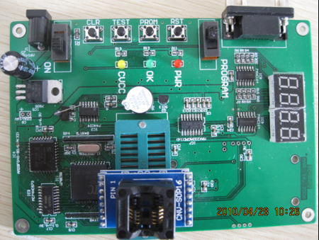
1. In PCB design and layout, follow the layout principle of “big first, then small, first difficult and then easy”, that is, important unit circuits and core components should be laid out first.
2. The principle block diagram should be referred to in the layout, and the main components should be arranged according to the main signal flow of the board.
3. The arrangement of components should be convenient for debugging and maintenance, that is, large components cannot be placed around small components, components that need to be debugged, and there must be enough space around the components.
4. For the circuit parts of the same structure, use the "symmetrical" standard layout as much as possible;
5. Optimize the layout according to the standards of uniform distribution, balanced center of gravity, and beautiful layout;
6. The same type of plug-in components should be placed in one direction in the X or Y direction. The same type of polarized discrete components should also strive to be consistent in the X or Y direction to facilitate production and inspection.
7. The heating elements should generally be evenly distributed to facilitate the heat dissipation of the veneer and the whole machine. Temperature sensitive devices other than the temperature detection element should be kept away from the components that generate large amounts of heat.
8. The layout should meet the following requirements as far as possible: the total connection is as short as possible, and the key signal line is the shortest; high voltage, high current signal and low current, low voltage weak signal are completely separated; analog signal and digital signal are separated; high frequency signal Separate from low-frequency signals; the spacing of high-frequency components should be sufficient.

It is time for PCB board inspection to pay attention to some details. In order to better ensure the quality of the product, the following common sense should be paid attention to when testing the PCB board.
1. It is strictly forbidden to use grounding test equipment to touch the TV, audio, video and other equipment on the backplane to detect PCB boards without isolation transformers.
It is strictly forbidden to test TV, audio, video and other equipment directly without power isolation transformer and grounding equipment. Although the general recorder has a power transformer, when it comes to special TV or audio equipment with large output power or insufficient knowledge of the nature of the power supply used, it is first necessary to find out whether there is a chassis. Whether the machine is powered on. The TV, audio and other devices on the backplane are short-circuited by the power supply, which affects the integrated circuit and causes the failure to further expand.
2, check the PCB board should pay attention to the insulation performance of the soldering iron
It is not allowed to use a soldering iron for soldering. To confirm that the soldering iron is not charged, it is best to ground the soldering iron shell. MOS circuits should be more careful. It is safer to use 6~8V low-voltage circuit iron.
3. Before testing the PCB board, understand the working principle of integrated circuits and related circuits.
Before checking and repairing the integrated circuit, you must be familiar with the function of the integrated circuit used, the internal circuit, the main electrical parameters, the function of each pin, the normal voltage of the pin, the waveform and the working condition. Component principle of peripheral components. If the above conditions are met, analysis and inspection will be easier.
4, the test PCB board will not cause a short circuit between the pins
When using an oscilloscope probe to measure voltage or test waveforms, the test leads or probes should not be short-circuited between the pins of the IC due to slippage. It is best to measure the peripheral printed circuit that communicates directly with the pin. Any short circuit at any moment can easily damage the integrated circuit, and you should be more careful when testing flat-package CMOS integrated circuits.
Single-sided circuit board processing four-layer immersion gold medical board finished product
5, the internal resistance of the PCB tester is large
When measuring the DC voltage of the IC pins, a multimeter with an internal resistance greater than 20KΩ/V should be used. Otherwise, some pin voltages will have larger measurement errors.
6, PCB board testing should pay attention to the heat dissipation of the power integrated circuit
The power integrated circuit should have good heat dissipation, and it is not allowed to work under high power without a heat sink.
7, the detection of PCB board leads should be reasonable
If it is necessary to add external components inside the integrated circuit instead of damaging the components, small components should be selected, and the wiring should be reasonable to avoid unnecessary parasitic coupling, especially the grounding between the audio power amplifier integrated circuit and the integrated circuit. Preamplifier circuit. Finish.
8, check the PCB board to ensure the quality of soldering
It is welded firmly during the soldering process, and the accumulation of solder and porosity may cause solder joints. The soldering time is usually less than 3 seconds, and the power of the soldering iron is applied to the internal heat type of about 25W. The soldered integrated circuit should be checked carefully. It is best to use an ohmmeter to measure whether there is a short circuit between the pins, and confirm that there is no solder adhesion, and then turn on the power.