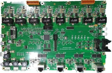
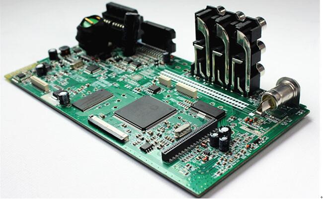
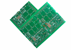
Standard for surface coating (plating) coating of PCB circuit boards
From the process and inspection of soldering components on PCB circuit board pads, the standard for surface coating (plating) coating on PCB circuit board pads mainly has the following five aspects.
• Heat resistance
At high welding temperatures, the surface coating (plating) coating can still protect the copper surface of the PCB circuit board pad from air oxidation and allow the soldering material to enter the copper (or metal) surface to establish a connection. The heat resistance of organic surface coating (plating) refers to the performance of its melting point and thermal decomposition (volatility) temperature. Its melting point should be close to or slightly lower than that of the PCB soldering material (tin), but its thermal decomposition The temperature (≥350°C) should be much higher than the melting point temperature and welding temperature of the welding material to ensure that the copper surface does not generate air oxidation during welding. The heat resistance of the metal surface coating layer does not have this problem.
• Coverage
For the organic heat-resistant solderability coating (including flux), it can be completely covered on the surface of the copper pad before and during the soldering process without being oxidized and polluted by air, only when the molten solder material is welded to the surface of the copper pad Then it can swim away, decompose and volatilize, and float (cover) on the surface of the solder joint.

Therefore, in order to ensure that the molten welding material is completely welded on the coupling disk, the surface tension of the molten organic surface coating layer must be low and the decomposition temperature must be high to ensure a good coverage before welding and during the process. At the same time, its specific gravity is much smaller than that of the molten solder material (tin) to ensure that the molten solder material squeezes and penetrates the copper surface. Therefore, the coverage of the organic surface coating refers to its temperature at the soldering temperature. Surface tension, specific gravity and other properties. The metal surface coating layer is partially melted into the welding material during welding or on the surface of the barrier layer to establish a connection.
• the remains
The residue of the organic heat-resistant solderability coating (plating) refers to the residue on the soldering pad or the solder joint after the soldering material is soldered. Under normal circumstances, these residues are hazardous (such as organic acids or halides, etc.) and should be removed, so cleaning measures should be taken after welding. Nowadays, there is no-clean welding technology, because the organic surface coating (plating) coating has very few residues after welding (most of them have been decomposed and volatilized).
• Corrosive
The corrosiveness of organic heat-resistant solderability coating (plating) coating refers to the corrosion of the surface of the PCB circuit board after the welding of the welding material, such as corrosion on the surface of the substrate of the PCB circuit board and the metal layer. This is because there are more or less halides or organic acids in the organic heat-resistant solderability coating (plating) (mainly to further clean the residual oxides and contaminants on the copper pad), but these The presence of acidic substances after welding is hazardous. In addition to decomposing and volatilizing, they must be cleaned and removed.
• Environmental protection
The environmental protection of the PCB surface coating (plating) coating refers to: the waste slag caused in the process of establishing the coating layer and the cleaned waste liquid after welding should be easy to dispose of, low cost and not polluting the environment.
PCB giant magnetoresistance effect and layer structure analysis
The so-called giant magnetoresistance effect refers to the phenomenon that the resistivity of a material changes significantly when there is an external magnetic field compared to when there is no external magnetic field. It is generally defined as GMR = where (H) is the resistivity of the material under the action of the magnetic field H (0) refers to the resistivity of the material without the action of an external magnetic field. The huge change in the resistance of some magnetic materials caused by an external magnetic field (called the giant magnetoresistance effect) is an important content in magnetoelectronics. There are many types of giant magnetoresistance materials with giant magnetoresistance effect at room temperature, for example, multilayer giant magnetoresistance materials, granular giant magnetoresistance materials, oxide giant magnetoresistance materials, tunnel junction magnetoresistance materials Wait.
The so-called magnetoresistance effect is a phenomenon in which the resistance of the conductor or semiconductor changes under the action of a magnetic field. The giant magnetoresistance effect was independently discovered by Peter Grünberg and Albert Fert in 1988., And they jointly won the 2007 Nobel Prize in Physics. Studies have found that in magnetic multilayer films such as Fe/Cr and Co/Cu, the ferromagnetic layers are separated by nano-thickness non-magnetic materials. Under certain conditions, the magnitude of the resistivity reduction is quite large, about 10 times higher than the magnetoresistance value of the usual magnetic metals and alloy materials. This phenomenon is called the "giant magnetoresistance effect."
The giant magnetoresistance effect can be explained by quantum mechanics. Every electron can spin, and the scattering rate of the electron depends on the spin direction and the magnetization direction of the magnetic material. The spin direction is the same as the magnetization direction of the magnetic material, the electron scattering rate is low, and more electrons pass through the magnetic layer, thus showing low impedance. Conversely, when the spin direction is opposite to the magnetization direction of the magnetic material, the electron scattering rate is high, so there are fewer electrons passing through the magnetic layer, which presents high impedance at this time.
Sensors based on PCB giant magnetoresistance effect mainly have three layers of sensing materials: Reference Layer or Pinned Layer, Normal Layer and Free Layer (The giant magnetoresistance effect often referred to as Free refers to the resistivity of raw materials). When there is an external magnetic field, there is a significant change compared to when there is no external magnetic field. It is usually defined as GMR = where (H) is the resistivity of the PCB material under the action of the magnetic field H (0) means that there is no external magnetic field. The resistivity of the lower raw material. The huge change in the resistance of some magnetic materials caused by an additional magnetic field (called the giant magnetoresistance effect) is an important content in magnetoelectronics. Giant magnets with a giant magnetoresistance effect at room temperature There are many types of resistance raw materials at this stage, for example, multilayer film giant magnetoresistance raw materials, granular giant magnetoresistance raw materials, oxide type giant magnetoresistance raw materials, tunnel junction magnetoresistance raw materials, etc.