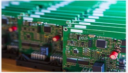
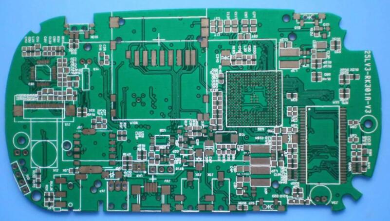
1 PCB design requires a planned design
Although Protel has the function of automatic planning, it cannot fully meet the working requirements of high-frequency circuit boards. It often depends on the designer's experience and according to the detailed situation. Planning to complete the overall design of the PCB circuit board. Whether the planning is reasonable or not directly affects the product's life, stability, EMC (electromagnetic compatibility), etc., it is necessary to start from the overall planning of the circuit board, the operability of the wiring and the manufacturability of the PCB, mechanical structure, heat dissipation, EMI (electromagnetic compatibility), etc. Comprehensive consideration in terms of interference), reliability, and signal integrity.
Generally, first place the components at a fixed position related to the mechanical size, then place the special and larger components, and finally place the small components. At the same time, it is necessary to coordinate the requirements of wiring, the placement of high-frequency components should be as compact as possible, and the wiring of signal lines should be as short as possible, so as to reduce the interference of signal lines.
1.1 The placement of the positioning plug-in related to the mechanical size
Power sockets, switches, interfaces between PCBs, indicator lights, etc. are all positioning plug-ins related to mechanical dimensions. Generally, the interface between the power supply and the PCB is placed at the edge of the PCB, and there should be a distance of 3 mm to 5 mm from the edge of the PCB; indicating that the light-emitting diodes should be placed accurately according to the needs; switches and some fine-tuning components, such as adjustable Inductance, adjustable resistance, etc. should be placed close to the edge of the PCB to facilitate adjustment and connection; components that require frequent changes must be placed in a relatively small location for easy replacement.
1.2 Placement of special components
High-power tubes, transformers, rectifier tubes and other heating devices generate more heat when working in high-frequency conditions, so you should think about ventilation and heat dissipation when planning, and place these components on the PCB where air is easy to circulate. . The high-power rectifier tube and adjustment tube should be equipped with a radiator and kept away from the transformer. Heat-sensitive components such as electrolytic capacitors should also be kept away from heating devices, otherwise the electrolyte will be dried, resulting in increased resistance and poor performance, which will affect the stability of the circuit.
Components that are prone to failure, such as adjustment tubes, electrolytic capacitors, relays, etc., should be considered for easy maintenance when placing them. For test points that often need to be measured, care should be taken to ensure that the test rods can be easily accessed when arranging components.
Since a 50 Hz leakage magnetic field is generated inside the power supply device, when it is cross-connected with some parts of the low-frequency amplifier, it will interfere with the low-frequency amplifier. Therefore, it is necessary to separate them or stop shielding treatment. It is best to arrange all levels of the amplifier in a straight line according to the schematic diagram. The advantage of this arrangement is that the ground current of each level is closed and active at this level and does not affect the work of other circuits. The input stage and output stage should be as far away as possible to reduce the parasitic coupling interference between them.
Considering the signal transmission relationship between the functional circuits of each unit, the low-frequency circuit and the high-frequency circuit should be separated, and the analog circuit and the digital circuit should be separated. The integrated circuit should be placed in the center of the PCB so that each pin can be connected to the wiring of other devices.
Devices such as inductors and transformers have magnetic coupling and should be placed orthogonally to each other to reduce magnetic coupling. In addition, they all have a strong magnetic field, and there should be an appropriately large space or magnetic shielding around them to reduce the impact on other circuits.
Appropriate high-frequency decoupling capacitors should be configured on the key parts of the PCB. For example, an electrolytic capacitor of 10 μF ~ 100 μF should be connected to the input end of the PCB power supply, and a ceramic of about 0.01 pF should be connected to the power supply pin of the integrated circuit. Chip capacitors. Some circuits must be equipped with appropriate high-frequency or low-frequency chokes to reduce the influence between the upper and lower frequency circuits. This point should be considered when designing and drawing the schematic, otherwise it will also affect the performance of the circuit.
The spacing between the components should be appropriate, and the spacing should be considered whether there is a possibility of breakdown or ignition between them.
For amplifiers containing push-pull circuits and bridge circuits, attention should be paid to the symmetry of the electrical parameters of the components and the symmetry of the structure, so that the dispersion parameters of the symmetrical components are as different as possible.
After the manual planning of the main components is completed, the method of component locking should be adopted so that these components will not move during the automatic planning. That is, execute the Edit change command or select Locked in the Properties of the component to lock it and no longer move it.
1.3 Placement of common components
Regarding common components, such as resistors, capacitors, etc., you should think about the arrangement of components, the size of the occupied space, the operability of wiring, and the convenience of welding. Automatic planning can be used.

2 Wiring design
Wiring is the overall request for high-frequency PCB design to be completed on the basis of reasonable planning. Wiring includes automatic wiring and manual wiring. Generally, regardless of the number of key signal lines, first stop the manual wiring of these signal lines. After the wiring is completed, stop the careful inspection of these signal lines. After the inspection, fix them, and then stop the automatic wiring of other wiring. That is, the manual and automatic wiring are separated to complete the wiring of the PCB.
Special attention should be paid to the following aspects in the process of high-frequency PCB wiring.
2.1 The trend of wiring
The wiring of the circuit is best to use a full straight line in accordance with the flow of the signal, and it can be completed with a 45° broken line or arc curve when changing the machine, which can reduce the external emission and mutual coupling of high-frequency signals. The wiring of high-frequency signal lines should be as short as possible. According to the operating frequency of the circuit, the length of the signal line wiring should be selected reasonably, which can reduce the spreading parameters and reduce the loss of the signal. When manufacturing a double-sided board, the wiring on two adjacent levels is best to be perpendicular, oblique or curved to intersect each other. Prevent each other from being parallel, so as to reduce mutual interference and parasitic coupling.
High-frequency signal lines and low-frequency signal lines should be separated as much as possible, and shielding measures should be taken if necessary to avoid mutual interference. Regarding the use of relatively weak signal input terminals, it is susceptible to interference from external signals. Ground wire can be used as a shield to surround it or to shield high-frequency connectors. Parallel wiring should be prevented on the same level, otherwise it will introduce scattered parameters and affect the circuit. If it cannot be prevented, a grounded copper foil can be introduced between the two parallel wires to form an isolated wire.
In digital circuits, the differential signal lines should be routed in pairs, try to make them parallel and close, and the length is not much different.
2.2 Wiring method
In the PCB wiring process, the minimum width of the trace is determined by the adhesion strength between the wire and the insulating substrate and the current intensity flowing through the wire. When the thickness of the copper foil is 0.05mm and the width is 1mm to 1.5mm, it can pass 2A current. The temperature will not be higher than 3 degree Celsius. Except for some special traces, the width of other traces on the same level should be as different as possible. The spacing of wiring in high-frequency circuits will affect the size of the scattered capacitance and inductance, thereby affecting signal loss, circuit stability, and signal interference. In high-speed switching circuits, the spacing of the wires will affect the transmission time of the signal and the quality of the waveform. Therefore, the minimum spacing of wiring should be greater than or equal to 0.5 mm, as long as it is allowed, it is better to use a relatively wide line for PCB wiring.
There should be a certain distance between the printed wire and the edge of the PCB (not less than the thickness of the board), which not only facilitates the installation and stop mechanical processing, but also improves the insulation performance.
When wiring a circuit that can only be connected by winding a large circle, flying wires should be used, that is, short wires should be used directly to reduce the interference caused by long-distance wiring.
Circuits containing magneto-sensitive components are more sensitive to surrounding magnetic fields, and when high-frequency circuits work, the corners of the wiring are likely to radiate electromagnetic waves. If magneto-sensitive components are placed in the PCB, ensure that the wiring corners are separated from them.
The wiring on the same level is not allowed to be interspersed. Regarding the lines that may be interspersed, you can use the method of "drilling" and "winding", that is, let a lead "drill" through the gap under the pins of other devices such as resistors, capacitors, and triodes, or from a line that may be interspersed. One end of the lead "winds around". In special circumstances, if the circuit is very complicated, in order to simplify the design, it is also allowed to use wire jumpers to deal with the interpenetration problem.
When the working frequency of the high-frequency circuit is high, it is also necessary to think about the impedance matching of the wiring and the antenna effect.
2.3 Wiring requirements for power cord and ground wire
According to the size of different working currents, try to enlarge the width of the power line. The high-frequency PCB should try to use a large area ground wire and plan it on the edge of the PCB to reduce the interference of external signals on the circuit; at the same time, the ground wire of the PCB can be well contacted with the shell, so that the ground voltage of the PCB is closer to Earth voltage. The central connection should be selected according to the detailed conditions. It is different from the low-frequency circuit. The grounding wire of the high-frequency circuit should be grounded nearby or multi-point grounding. The grounding wire should be short and thick to minimize the ground impedance. The allowable current request can be Reach the specification of 3 times the working current. The grounding wire of the speaker should be connected to the grounding point of the output stage of the PCB power amplifier. Do not ground it arbitrarily.
In the wiring process, some reasonable wiring should be locked in time to avoid repeated wiring. That is, execute the EditselectNet command and select Locked in the properties of the pre-wiring to lock it and no longer move it.
3 PCB pad and copper design
3.1 Land and aperture
Under the condition of ensuring that the minimum wiring spacing does not violate the designed electrical spacing, the design of the pad should be larger to ensure sufficient ring width. The inner hole of the ordinary pad is slightly larger than the lead diameter of the component, and the design is too large, and it is easy to form a virtual solder during soldering. The outer diameter D of the pad is generally not less than (d+1.2)mm, where d is the inner diameter of the pad. For some PCBs with relatively high density, the minimum value of the pad can be (d+1.0) mm. The shape of the pad is usually set to be circular, but the pad of the integrated circuit of the DIP package is preferably a racetrack shape, so that the area of the pad can be increased in a limited space, which is beneficial to the welding of the integrated circuit. The connection between the wiring and the pad should be smoothly transitioned, that is, when the width of the wiring into the round pad is smaller than the diameter of the round pad, the teardrop design should be adopted.
It should be noted that the size of the aperture d in the pad is different, and it should be considered based on the size of the lead diameter of the actual component, such as component holes, device holes, and slot holes. The hole spacing of the pads should also be considered based on the device method of the practical components. For example, resistors, diodes, tubular capacitors and other components have "vertical" and "horizontal" installation methods. The hole distances of these two methods are different. In addition, the design of the pad hole distance must also consider the minimum gap requirements between components, especially the gap requirements between special components are guaranteed by the hole distance between the pads.
In high-frequency PCBs, the number of vias should also be minimized, which can reduce the scattered capacitance and increase the mechanical strength of the PCB. In short, in the design of high-frequency PCB, the design of the pad and its shape, aperture and pitch must not only consider its particularity, but also meet the requirements of the consumer process. The use of standardized design can not only reduce product costs, but also improve the efficiency of consumption while ensuring the quality of production.
3.2 Copper coating
The main purpose of copper coating is to improve the anti-interference ability of the circuit. At the same time, it has great benefits in terms of PCB heat dissipation and PCB strength. Copper coating and grounding can also play a shielding role. However, large-area strip copper foil cannot be used. Because a large amount of heat will be generated when the PCB is used for too long, the strip copper foil is prone to shrinkage and scattered phenomena at this time. Therefore, it is best to use grids when depositing copper. The grid is connected to the grounding network of the circuit, so that the grid will have a better shielding effect. The size of the grid network is determined by the interference frequency to be shielded.
After completing the design of wiring, pads and vias, DRC (Design Rule Check) should be performed. In the inspection results, the differences between the designed diagram and the defined rules are listed in detail, and the network that does not meet the request can be found. However, you should first stop the DRC parameter setting before wiring to run the DRC, that is, execute the ToolsDesign Rule Check command.
4 Conclusion
The high-frequency circuit PCB design is a complicated process, and many elements are touched, which may be directly related to the working performance of the high-frequency circuit. Therefore, designers need to study and explore from time to time in practical work, accumulate experience from time to time, and separate the new EDA (Electronic Design Automation) technology to design high-frequency circuit PCBs with excellent performance.