What details should be paid attention to in the PCB design reverse schematic diagram?
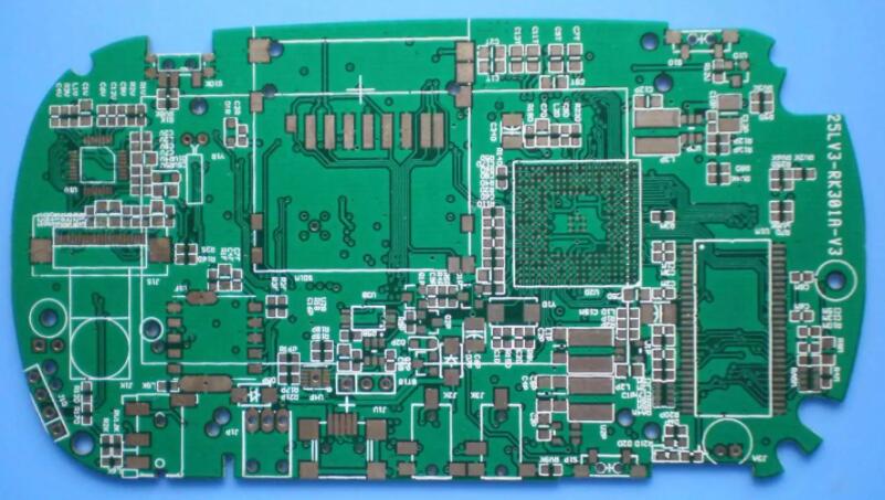
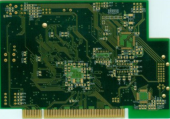
General product research and development must first carry out the schematic design, and then carry out the PCB design according to the schematic. Reversing the schematic diagram refers to inversely pushing out the PCB circuit diagram based on the PCB document diagram or directly depicting the PCB circuit diagram based on the actual product. So, what should be paid attention to in the process of PCB design to reverse the schematic diagram?
1. Reasonable division of functional areas
In the reverse design of the schematic diagram of the PCB circuit board, a reasonable division of the functional area can improve the drawing efficiency. Generally speaking, components with the same function on a PCB circuit board will be arranged in a concentrated manner, and dividing the area by function can have a convenient and accurate basis when inverting the schematic diagram. First, find out the core components in a certain functional unit, and then according to the wiring connection, you can find other components of the same functional unit to form a functional partition. In addition, in this process, the serial numbers of the components on the circuit board should be used cleverly to help you partition the functions faster.
Second, find the right reference parts
After determining the reference parts, drawing according to the pins of these reference parts can ensure the accuracy of the schematic diagram to a greater extent. Under normal circumstances, you can choose components that play a major role in the circuit as reference components. They are generally larger in size and have more pins, which are convenient for drawing. Such as integrated circuits, transformers, transistors, etc., can be used as suitable components. Benchmark parts.

3. Correctly distinguish lines and draw wiring reasonably
The distinction between ground wire, power wire and signal wire can be analyzed in terms of the connection of components, the width of the copper foil of the circuit, and the characteristics of the electronic product itself. In the wiring drawing, in order to avoid the crossing and interpenetration of lines, a large number of grounding symbols can be used for the grounding line. Various lines can use lines of different colors to ensure that they are clear and identifiable. Special signs can be used for various components, and even the unit circuits can be separated. Draw, and finally combine.
4. Master the basic framework and learn from similar schematic diagrams
It is not only necessary to directly draw the basic forms of some simple and classic unit circuits, but also to form the overall framework of electronic circuits. In addition, based on the accumulation of experience, we can fully learn from similar circuit diagrams to reverse the schematic diagrams of new products.
Five, verification and optimization
After the schematic drawing is completed, the reverse design of the PCB schematic can be said to be completed after testing and verification. According to the PCB document drawing, the schematic diagram is compared, analyzed and checked to ensure that the schematic diagram is completely consistent with the document diagram. If the layout of the schematic diagram is found to be inconsistent with the requirements during the check, the schematic diagram will need to be adjusted.
The above are the details that should be paid attention to in the reverse design of PCB design. Do you understand it?