When the PCB has a lot of ground, it can be used as a reference and independently covered according to the position of the PCB circuit board of Jinbei to distinguish between digital and analog. It is also possible to use zero-ohm resistance or magnetic beads or inductors to connect single-point connections to different grounds.

2. Because the crystal oscillator in the circuit is a high-frequency emission source, the cover near the crystal oscillator needs to surround the crystal oscillator cover, and then the crystal oscillator housing needs to be grounded separately. Vias can be added to the islanding problem, but not all can be so, it needs to be realistic.
3. At the beginning of the wiring, the ground wire is treated the same, and the wiring rules should be paid attention to. You cannot rely on the addition of vias to remove the ground pins for the connection after covering, which will affect the effect of the PCB circuit board. In addition, the board of the PCB circuit board needs to be 180 degrees horizontal, because from the perspective of electromagnetics, sharp corners will form the transmitting antenna, it is recommended to use the edge of the arc to avoid influence.
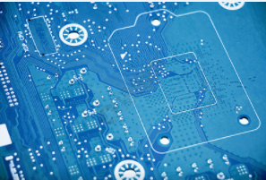
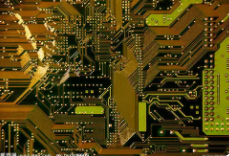
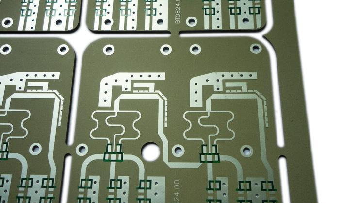
Precautions for covering in PCB circuit board design
4. It is more convenient to handle the open area of the middle layer of the multilayer board without covering the wiring, and the metal inside the device, the metal radiator, the reinforcement bar, the heat dissipation metal block of the three-terminal regulator, and the grounding isolation belt near the crystal oscillator need to be good. Grounded.
In summary, the grounding problem can be found to be very important in the precautions in the above PCB circuit board design. The PCB circuit board grounding problem is handled in place and covered well, which can not only reduce the voltage and improve the utilization efficiency of the power supply; connect with the ground wire can reduce the ground wire impedance; it can also reduce the loop area. In addition, the PCB circuit board covering is also very helpful for not deforming the PCB during soldering.
At present, the country has higher and higher requirements for environmental protection and greater efforts in link governance. This is a challenge but also an opportunity for PCB factories. If PCB factories are determined to solve the problem of environmental pollution, then FPC flexible circuit board products can be at the forefront of the market, and PCB factories can get opportunities for further development.
The Internet era has broken the traditional marketing model, and a large number of resources have been gathered together to the greatest extent through the Internet, which has also accelerated the development speed of FPC flexible circuit boards, and then as the development speed accelerates, environmental problems will continue to appear in PCB factories. In front of him. However, with the development of the Internet, environmental protection and environmental informatization have also been developed by leaps and bounds. Environmental information data centers and green electronic procurement are gradually being applied to the actual production and operation fields.