What are the precautions for PCB circuit board design?
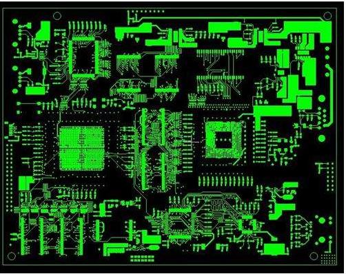
PCB factory: Designing a circuit is a hard work that electronic engineers must master. If the circuit board is designed unreasonably, the performance will be greatly reduced, and it may even not work properly in severe cases. So, what are the precautions for PCB circuit board design?
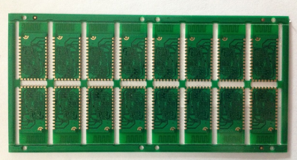
1. Make a physical border
The closed physical frame is very important for the future component layout and wiring, and it must be accurate, otherwise installation problems will occur in the future. It is best to use arcs at the corners. On the one hand, it can avoid sharp corners from scratching workers, and at the same time, it can reduce the effect of stress.
2. Layout of components
The layout and wiring of components have a great influence on the quality of the product. The following principles should be followed:
(1) Placement order
First place the components related to the structure at a fixed position, such as power sockets, indicator lights, switches, connectors, etc.; then place special components and large components on the line, such as heating components, transformers, ICs, etc. Finally, place the small device.
(2) Pay attention to heat dissipation
For high-power circuits, the heating elements should be placed as close to the side as possible to facilitate heat dissipation, and do not concentrate in one place.

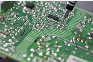
3. Reasonable wiring
The following wiring principles should be followed:
(1) High-frequency digital circuit traces should be thinner and shorter;
(2) Attention should be paid to isolation between large current signals, high voltage signals and small signals;
(3) In double-panel wiring, the wires on both sides should be perpendicular to each other, obliquely crossing, or bent to avoid parallel to each other to reduce parasitic coupling;
(4) The wiring corner should be greater than 90 degrees as much as possible, and corners below 90 degrees should be avoided;
(5) The same address line or data line, the length of the trace should not be too different;
(6) Try to walk the wire on the soldering surface; use as few vias and jumpers as possible;
(7) The components and wiring should not be placed too close to the side;
(8) The convenience of production, debugging and maintenance must be considered
4. Perfect adjustment
After completing the wiring, all you have to do is to make some adjustments to the text, individual components, wiring, and copper. If you use copper instead of the ground wire, you must pay attention to whether the entire ground is connected, the current size, flow direction, and whether there are special requirements to ensure that unnecessary errors are reduced.
5. Check the network
Sometimes the network relationship of the circuit board drawn is different from the schematic diagram due to negligence. At this time, it is necessary to check and verify.
6. Use the simulation function
Doing so can find some problems in advance and greatly reduce the amount of debugging work in the future.
The above are the precautions in PCB circuit board design summarized by professional PCB engineers based on years of experience. I hope it can give you some enlightenment.