Printed circuit board {PCB}, also known as printed circuit board, is a provider of electrical connections for electronic components. Its development has a history of more than 100 years; its design is mainly layout design; the main advantage of using circuit boards is to greatly reduce wiring and assembly errors, and improve the level of automation and production labor.
Since the printed circuit board is not a general terminal product, the definition of the name is a little confusing. For example, the motherboard used in personal computers is called the main board, and cannot be directly called the circuit board. Although there are circuit boards in the main board, They are not the same, so when evaluating the industry, the two are related but cannot be said to be the same. Another example: because there are integrated circuit parts mounted on the circuit board, the news media call it an IC board, but in fact it is not equivalent to a printed circuit board. We usually say that the printed circuit board refers to the bare board-that is, the circuit board without upper components.
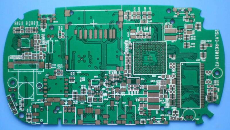
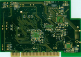
PCB circuit boards have developed from single-sided to double-sided, multi-layer, flexible and flexible, and still maintain their respective development trends. Due to the continuous development in the direction of high precision, high density and high reliability, continuous reduction in size, cost reduction, and performance improvement, the printed board will still maintain a strong vitality in the development of electronic equipment in the future.
So how is the PCB circuit board designed? After reading the following seven steps, you will understand
1. Preliminary preparation
Including the preparation of components and schematic diagrams. Before proceeding with PCB design, we must first prepare the schematic SCH components and PCB component packaging library.
The PCB component package library is best established by the engineer based on the standard size data of the selected device. In principle, establish the PC component package library first, and then establish the schematic SCH component library.
PCB component package library requirements are high, which directly affects the installation of PCB; schematic diagram SCH component library requirements are relatively loose, but pay attention to define the pin attributes and the corresponding relationship with the PCB component package library.
2. PCB structure design
According to the determined PCB circuit board size and various mechanical positioning, draw the PCB frame in the PCB design environment, and place the required connectors, buttons/switches, positioning holes, assembly holes, etc. according to the positioning requirements.
Fully consider and determine the wiring area and non-wiring area (such as how much area around the positioning hole belongs to the non-wiring area).
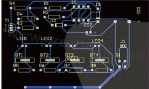
The layout design is to place the components in the PCB frame according to the design requirements. Generate the netlist (Design-Create Netlist) in the schematic tool, and then import the netlist (Design-Import Netlist) in the PCB software. After the netlist is successfully imported, it will exist in the background of the software. Through the Placement operation, all devices can be called out, and there is a flying line prompt connection between the pins. At this time, the layout design of the device can be carried out.
PCB layout design is the first important process in the entire PCB design process. The more complex the PCB board, the better the layout can directly affect the difficulty of later wiring.
Layout design relies on the PCB circuit board designer's basic circuit knowledge and rich design experience, which is a higher level requirement for the PCB circuit board designer. Elementary circuit board designers have little experience and are suitable for small module layout design or PCB layout design tasks with lower overall board difficulty.
4. PCB wiring design

PCB layout design is the process with the largest workload in the entire PCB design, which directly affects the performance of the PCB board.
In the PCB design process, wiring generally has three realms:
The first is layout, which is the most basic entry requirement for PCB design;
The second is the satisfaction of electrical performance, which is a standard to measure whether a PCB board is qualified. After the wiring is laid out, carefully adjust the wiring to achieve the best electrical performance;
Thirdly, neat and beautiful, chaotic wiring, even if the electrical performance is passed, it will cause great inconvenience to the later modification of the board optimization and testing and maintenance. The wiring requirements are neat and uniform, and they cannot be crisscrossed and disordered.
5. Wiring optimization and silk screen placement
"PCB design is not the best, only better", "PCB design is an art of defects", this is mainly because PCB design needs to realize the design requirements of all aspects of hardware, and individual requirements may be in conflict with each other. Bear's paw can't have both.
6. Network DRC inspection and structure inspection
Quality control is an important part of the PCB design process. General quality control methods include: design self-inspection, design mutual inspection, expert review meetings, special inspections, etc.
Schematic diagrams and structural element diagrams are the most basic design requirements. Network DRC inspection and structural inspection are to confirm that the PCB design meets the two input conditions of the schematic netlist and structural element diagram.
Generally, circuit board designers will have their own accumulated design quality check Checklist, where the entries partly come from the company or department's specifications, and the other part comes from their own experience summaries. Special inspections include Valor inspection and DFM inspection of the design. These two parts focus on the PCB design and output back-end processing gerber files.
7. PCB system board
Before the PCB is officially processed and made, the PCB circuit board designer needs to communicate with the PE of the PCB supplier to answer the manufacturer's confirmation questions about the PCB board processing.
This includes but is not limited to: selection of PCB board model, adjustment of circuit layer line width and line spacing, adjustment of impedance control, adjustment of PCB stacking thickness, surface treatment processing technology, aperture tolerance control and delivery standards, etc.